Anterwell Technology Ltd.
Anterwell Technology Ltd.
Large Original stock of IC Electronics Components, Transistors, Diodes etc.
High Quality, Reasonable Price, Fast Delivery.
Anterwell Technology Ltd.
Large Original stock of IC Electronics Components, Transistors, Diodes etc.
High Quality, Reasonable Price, Fast Delivery.


|
Product Details:
Payment & Shipping Terms:
|
| Max Offset Voltage: | 75 MV | Max Offset Voltage Drift: | 1 μV/℃ |
|---|---|---|---|
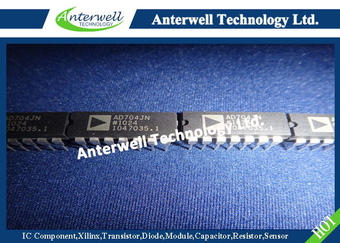
| Max Input Bias Current: | 150 PA | Package: | DIP-14 |
| Highlight: | low voltage power mosfet,hybrid inverter circuit |
||
Quad Picoampere Input Current Bipolar Op Amp AD704
FEATURES CONNECTION DIAGRAMS
High DC Precision
75 mV max Offset Voltage ![]()
1 mV/8C max Offset Voltage Drift
150 pA max Input Bias Current
0.2 pA/8C typical IB Drift
Low Noise
0.5 mV p-p typical Noise, 0.1 Hz to 10 Hz
Low Power
600 mA max Supply Current per Amplifier
Chips & MIL-STD-883B Processing Available
Available in Tape and Reel in Accordance
with EIA-481A
Standard Single Version: AD705, Dual Version: AD706
PRIMARY APPLICATIONS
Industrial/Process Controls
Weigh Scales
ECG/EKG Instrumentation
Low Frequency Active Filters
PRODUCT DESCRIPTION
The AD704 is a quad, low power bipolar op amp that has the low input bias current of a BiFET amplifier but which offers a significantly lower IB drift over temperature. It utilizes Superbeta bipolar input transistors to achieve picoampere input bias current levels (similar to FET input amplifiers at room temperature), while its IB typically only increases by 5× at +125°C (unlike a BiFET amp, for which IB doubles every 10°C resulting in a 1000× increase at +125°C). Furthermore the AD704
achieves 75 µV offset voltage and low noise
characteristics of a precision bipolar input op amp.
![]() Since it has only 1/20 the input bias current of an AD OP07, the AD704 does not require the commonly used “balancing” resistor. Furthermore, the current noise is 1/5 that of the AD OP07 which makes the AD704 usable with much higher source impedances. At 1/6 the supply current (per amplifier) of the AD OP07, the AD704 is better suited for today’s higher density circuit boards and battery powered applications. The AD704 is an excellent choice for use in low frequency active filters in 12- and 14-bit data acquisition systems, in precision instrumentation, and as a high quality integrator. The AD704 is internally compensated for unity gain and is available in five performance grades. The AD704J and AD704K are rated over the commercial temperature range of 0°C to +70°C. The AD704A and AD704B are rated over the industrial temperature of –40°C to +85°C. The AD704T is rated over the military temperature range of –55°C to +125°C and is available processed to MIL- STD-883B, Rev. C.
Since it has only 1/20 the input bias current of an AD OP07, the AD704 does not require the commonly used “balancing” resistor. Furthermore, the current noise is 1/5 that of the AD OP07 which makes the AD704 usable with much higher source impedances. At 1/6 the supply current (per amplifier) of the AD OP07, the AD704 is better suited for today’s higher density circuit boards and battery powered applications. The AD704 is an excellent choice for use in low frequency active filters in 12- and 14-bit data acquisition systems, in precision instrumentation, and as a high quality integrator. The AD704 is internally compensated for unity gain and is available in five performance grades. The AD704J and AD704K are rated over the commercial temperature range of 0°C to +70°C. The AD704A and AD704B are rated over the industrial temperature of –40°C to +85°C. The AD704T is rated over the military temperature range of –55°C to +125°C and is available processed to MIL- STD-883B, Rev. C.
| Model | Conditions |
AD704J/A Min Typ Max |
AD704K/B Min Typ Max |
AD704T Min Typ Max |
Units |
|
INPUT OFFSET VOLTAGE Initial Offset Offset vs. Temp, Average TC vs. Supply (PSRR) TMIN–TMAX Long Term Stability |
TMIN–TMAX
VS = ±2 to ±18 V VS = ±2.5 to ±18V
|
50 150 100 250 0.2 1.5 100 132 100 126 0.3 |
30 75 50 150 0.2 1.0 112 132 108 126 0.3 |
30 100 80 150 1.0 112 132 108 126 0.3 |
µV µV µV/°C dB dB µV/month |
|
INPUT BIAS CURRENT1
vs. Temp, Average TC TMIN–TMAX TMIN–TMAX |
VCM = 0 V VCM = ±13.5 V
VCM = 0 V VCM = ±13.5 V |
100 270 300 0.3 300 400 |
80 150 200 0.2 200 300 |
80 200 250 1.0 600 700 |
pA pA pA/°C pA pA |
|
INPUT OFFSET CURRENT
vs. Temp, Average TC TMIN–TMAX TMIN–TMAX |
VCM = 0 V VCM = ±13.5 V
VCM = 0 V VCM = ±13.5 V |
80 250 300 0.6 100 300 100 400 |
30 100 150 0.4 80 200 80 300 |
50 150 200 0.4 80 400 100 500 |
pA pA pA/°C pA pA |
|
MATCHING CHARACTERISTICS Offset Voltage
Input Bias Current2
Common-Mode Rejection3
Power Supply Rejection4
Crosstalk5 |
TMIN–TMAX
TMIN–TMAX
TMIN–TMAX
TMIN–TMAX f = 10 Hz RLOAD = 2 kΩ |
250 400 500 600 94 94 94
150 |
130 200 300 400 110 104 110 106
150 |
150 250 400 600 104 104 110 106
150 |
µV µV pA pA dB dB dB dB
dB |
|
FREQUENCY RESPONSE UNITY GAIN Crossover Frequency Slew Rate, Unity Gain Slew Rate |
G = –1 TMIN–TMAX |
0.8 0.15 0.1 |
0.8 0.15 0.1 |
0.8 0.15 0.1 |
MHz V/µs V/µs |
|
INPUT IMPEDANCE Differential Common-Mode |
40‖2 300‖2 |
40‖2 300‖2 |
40‖2 300‖2 |
MΩ‖pF GΩ‖pF |
|
|
INPUT VOLTAGE RANGE Common-Mode Voltage Common-Mode Rejection Ratio |
VCM = ±13.5 V TMIN–TMAX |
±13.5 ±14 100 132 98 128 |
±13.5 ±14 114 132 108 128 |
±13.5 ±14 110 132 108 128 |
V dB dB |
| INPUT CURRENT NOISE |
0.1 to 10 Hz f = 10 Hz |
3 50 |
3 50 |
3 50 |
pA p-p fA/√Hz |
| INPUT VOLTAGE NOISE | 0.1 to 10 Hz
f = 10 Hz f = 1 kHz |
0.5 17 15 22 |
0.5 2.0 17 15 22 |
0.5 2.0 17 15 22 |
µV p-p nV/√Hz nV/√Hz |
| OPEN-LOOP GAIN |
VO = ±12 V RLOAD = 10 kΩ TMIN–TMAX VO = ±10 V RLOAD = 2 kΩ TMIN–TMAX |
200 2000 150 1500
200 1000 150 1000 |
400 2000 300 1500
300 1000 200 1000 |
400 2000 300 1500
200 1000 100 1000 |
V/mV V/mV
V/mV V/mV |
|
OUTPUT CHARACTERISTICS Voltage Swing
Current |
RLOAD = 10 kΩ TMIN–TMAX Short Circuit |
±13 ±14 ±15 |
±13 ±14 ±15 |
±13 ±14 ±15 |
V mA |
|
CAPACITIVE LOAD Drive Capability |
Gain = + 1 |
10,000 |
10,000 |
10,000 |
pF |
|
POWER SUPPLY Rated Performance Operating Range Quiescent Current
|
TMIN–TMAX |
±15 ±2.0 ±18 1.5 2.4 1.6 2.6 |
±15 ±2.0 ±18 1.5 2.4 1.6 2.6 |
±15 ±2.0 ±18 1.5 2.4 1.6 2.6 |
V V mA mA |
| TRANSISTOR COUNT | # of Transistors | 180 | 180 | 180 |
NOTES
1 Bias current specifications are guaranteed maximum at either input.
2 Input bias current match is the maximum difference between corresponding inputs of all four amplifiers.
3 CMRR match is the difference of ∆VOS/∆VCM between any two amplifiers, expressed in dB.
4 PSRR match is the difference between ∆VOS/∆VSUPPLY for any two amplifiers, expressed in dB.
5 See Figure 2a for test circuit.
All min and max specifications are guaranteed.
Specifications subject to change without notice.
High Power Rectifier Diode 1N4756A , Silicon Planar Zener Diodes
Bridge Type Rectifier Diode 1N4007 50 to 1000 Volts 1.0 Ampere
1N4742A Silicon Planar Zener Diodes for Stabilized Power Supply
Power Programmable IC Chips XC6SLX100-3FGG484C Spartan-6 Family Overview
128K Bytes Sound IC Chip Programming ATMEGA128-16AU 8 Bit Microcontroller
EMC Programmable IC Chips Compliant Slew Rate Limited EI , Timer IC Chip
SMD Power Mosfet Module L7812CV TO-220 Power Trans Electronic Compoents
2SD1594 3 Pin Transistor NEC NPN Power Transistor Switching High Speed
2N5459 Power Mosfet Transistor N-Channel To-92 Original Stock FSC