Anterwell Technology Ltd.
Anterwell Technology Ltd.
Large Original stock of IC Electronics Components, Transistors, Diodes etc.
High Quality, Reasonable Price, Fast Delivery.
Anterwell Technology Ltd.
Large Original stock of IC Electronics Components, Transistors, Diodes etc.
High Quality, Reasonable Price, Fast Delivery.


Product Details:
Payment & Shipping Terms:
|
| Supply Voltage: | 3 To 3.6 V | Input High Voltage: Logic 1; All Inputs: | 2 To VDD + 0.3 V |
|---|---|---|---|
| Input Low Voltage: Logic 0; All Inputs: | -0.3 To 0.8 V | Input Leakage Current: | -5 To 5 µA |
| Storage Temperature (plastic): | -55°C To +150°C | Power Dissipation: | 1W |
| High Light: | electronics ic chip,integrated circuit ic |
||
128Mb: x4, x8, x16 SDRAM
SYNCHRONOUS DRAM
MT48LC32M4A2 – 8 Meg x 4 x 4 banks
MT48LC16M8A2 – 4 Meg x 8 x 4 banks
MT48LC8M16A2 – 2 Meg x 16 x 4 banks
FEATURES
• PC100-, and PC133-compliant
• Fully synchronous; all signals registered on positive edge of system clock
• Internal pipelined operation; column address can be changed every clock cycle
• Internal banks for hiding row access/precharge
• Programmable burst lengths: 1, 2, 4, 8, or full page
• Auto Precharge, includes CONCURRENT AUTO PRECHARGE, and Auto Refresh Modes
• Self Refresh Mode; standard and low power
• 64ms, 4,096-cycle refresh
• LVTTL-compatible inputs and outputs
• Single +3.3V ±0.3V power supply
OPTIONS MARKING
• Configurations
32 Meg x 4 (8 Meg x 4 x 4 banks) 32M4
16 Meg x 8 (4 Meg x 8 x 4 banks) 16M8
8 Meg x 16 (2 Meg x 16 x 4 banks) 8M16
• WRITE Recovery (t WR)
t WR = “2 CLK”1 A2
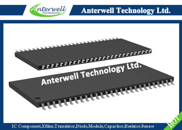
• Package/Pinout
Plastic Package – OCPL2
54-pin TSOP II (400 mil) TG
60-ball FBGA (8mm x 16mm) FB 3,6
60-ball FBGA (11mm x 13mm) FC 3,6
• Timing (Cycle Time)
10ns @ CL = 2 (PC100) -8E 3,4,5
7.5ns @ CL = 3 (PC133) -75
7.5ns @ CL = 2 (PC133) -7E
• Self Refresh
Standard None
Low power L
• Operating Temperature Range
Commercial (0℃ to +70℃) None
Industrial (-40℃ to +85℃) IT 3
Part Number Example: MT48LC16M8A2TG-7E
NOTE:
1. Refer to Micron Technical Note: TN-48-05.
2. Off-center parting line.
3. Consult Micron for availability.
4. Not recommended for new designs.
5. Shown for PC100 compatability. 6. See page 59 for FBGA Device Marking Table.
![]()
![]()
GENERAL DESCRIPTION
The Micron® 128Mb SDRAM is a high-speed CMOS, dynamic random-access memory containing 134,217,728 bits. It is internally configured as a quad-bank DRAM with a synchronous interface (all signals are registered on the positive edge of the clock signal, CLK). Each of the x4’s 33,554,432-bit banks is organized as 4,096 rows by 2,048 columns by 4 bits. Each of the x8’s 33,554,432-bit banks is organized as 4,096 rows by 1,024 columns by 8 bits. Each of the x16’s 33,554,432-bit banks is organized as 4,096 rows by 512 columns by 16 bits.
Read and write accesses to the SDRAM are burst oriented; accesses start at a selected location and continue for a programmed number of locations in a programmed sequence. Accesses begin with the registration of an ACTIVE command, which is then followed by a READ or WRITE command. The address bits registered coincident with the ACTIVE command are used to select the bank and row to be accessed (BA0, BA1 select the bank; A0-A11 select the row). The address bits registered coincident with the READ or WRITE command are used to select the starting column location for the burst access.
The SDRAM provides for programmable READ or WRITE burst lengths of 1, 2, 4, or 8 locations, or the full page, with a burst terminate option. An auto precharge function may be enabled to provide a selftimed row precharge that is initiated at the end of the burst sequence.
The 128Mb SDRAM uses an internal pipelined architecture to achieve high-speed operation. This architecture is compatible with the 2n rule of prefetch architectures, but it also allows the column address to be changed on every clock cycle to achieve a high-speed, fully random access. Precharging one bank while accessing one of the other three banks will hide the precharge cycles and provide seamless high-speed, random-access operation.
The 128Mb SDRAM is designed to operate in 3.3V memory systems. An auto refresh mode is provided, along with a power-saving, power-down mode. All inputs and outputs are LVTTL-compatible.
SDRAMs offer substantial advances in DRAM operating performance, including the ability to synchronously burst data at a high data rate with automatic columnaddress generation, the ability to interleave between internal banks in order to hide precharge time and the capability to randomly change column addresses on each clock cycle during a burst access.
ABSOLUTE MAXIMUM RATINGS*
Voltage on VDD/VDDQ Supply Relative to VSS ........................................... -1V to +4.6V
Voltage on Inputs, NC or I/O Pins Relative to VSS ........................................ -1V to +4.6V
Operating Temperature, TA (commercial)......................................................0°C to +70°C
Operating Temperature, TA (extended; IT parts) ...................................... -40°C to +85°C
Storage Temperature (plastic)................................................................. -55°C to +150°C
Power Dissipation ....................................................................................................... 1W
*Stresses greater than those listed under “Absolute Maximum Ratings” may cause permanent damage to the device. This is a stress rating only, and functional operation of the device at these or any other conditions above those indicated in the operational sections of this specification is not implied. Exposure to absolute maximum rating conditions for extended periods may affect reliability.
Stock Offer (Hot Sell)
| Part no. | Quantity | Brand | D/C | Package |
| LP2986IMX-5.0 | 3583 | NSC | 14+ | SOP-8 |
| MMBD914LT1G | 20000 | ON | 16+ | SOT-23 |
| OPA4131NJ | 7620 | TI | 14+ | SOP-14 |
| LPS3010-103MLC | 4509 | COILCRAF | 14+ | SMD |
| N80C152JA-1 | 4800 | INTEL | 16+ | PLCC |
| MC56F8257VLH | 3592 | FREESCALE | 15+ | LQFP |
| LTC1480IS8 | 5494 | LINEAR | 15+ | SOP |
| L6562ADTR | 10000 | ST | 15+ | SOP8 |
| MC56F8006VLC | 3568 | FREESCALE | 15+ | LQFP |
| MCP6542-I/SN | 5518 | MICROCHIP | 16+ | SOP |
| LPC11U14FBD48/201 | 5168 | NXP | 15+ | LQFP-48 |
| XCR3064XL-10VQG44C | 416 | XILINX | 14+ | QFP44 |
| MCF51JM128VLH | 4810 | FREESCALE | 15+ | LQFP |
| MC56F8006VLF | 3574 | FREESCALE | 14+ | QFP |
| LP38502SDX-ADJ | 1732 | NSC | 15+ | LLP-8 |
| LM392N | 10000 | NSC | 14+ | DIP-8 |
| MMSZ4680T1G | 20000 | ON | 10+ | SOD-123 |
| MAR-8ASM | 4734 | MINI | 14+ | SMT |
| LM336BZ-5.0 | 5022 | NSC | 13+ | TO-92 |
| MAR-8A+ | 3823 | MINI | 16+ | SMT |
| LM350TG | 780 | ON | 13+ | TO-220 |
| MJD32CT4G | 10000 | ON | 16+ | TO-252 |
| LM392MX | 6824 | NSC | 14+ | SOP-8 |
| MFI341S2164 | 6010 | KIT | 14+ | QFN |
| MC14LC5480DWR2 | 10388 | FREESCALE | 16+ | SOP |
| XP152A12COMR | 9000 | TOREX | 15+ | SOT23 |
| LNK605DG | 4507 | POWER | 15+ | DIP-7 |
| LP324MX | 5293 | NSC | 15+ | SOP-14 |
| MAX809ZD | 10000 | NXP | 12+ | SOT |
| CMX865AD4 | 1970 | CML | 14+ | SOP16 |
High Power Rectifier Diode 1N4756A , Silicon Planar Zener Diodes
Bridge Type Rectifier Diode 1N4007 50 to 1000 Volts 1.0 Ampere
1N4742A Silicon Planar Zener Diodes for Stabilized Power Supply
Power Programmable IC Chips XC6SLX100-3FGG484C Spartan-6 Family Overview
128K Bytes Sound IC Chip Programming ATMEGA128-16AU 8 Bit Microcontroller
EMC Programmable IC Chips Compliant Slew Rate Limited EI , Timer IC Chip
SMD Power Mosfet Module L7812CV TO-220 Power Trans Electronic Compoents
2SD1594 3 Pin Transistor NEC NPN Power Transistor Switching High Speed
2N5459 Power Mosfet Transistor N-Channel To-92 Original Stock FSC