Anterwell Technology Ltd.
Anterwell Technology Ltd.
Large Original stock of IC Electronics Components, Transistors, Diodes etc.
High Quality, Reasonable Price, Fast Delivery.
Anterwell Technology Ltd.
Large Original stock of IC Electronics Components, Transistors, Diodes etc.
High Quality, Reasonable Price, Fast Delivery.


Product Details:
Payment & Shipping Terms:
|
| Maximum Junction Temperature: | +125 ° C | Maximum Soldering Temperature: | +220 ° C |
|---|---|---|---|
| Storage Temperature (ambient): | –65 To 150 ° C | Internal Supply Voltage Relative To GND: | –0.5 To 1.32 V |
| Auxiliary Supply Voltage Relative To GND: | –0.5 To 3.0 V | Key Memory Battery Backup Supply: | –0.5 To 4.05 V |
| Highlight: | ic programmer circuit,programmable audio chip |
||
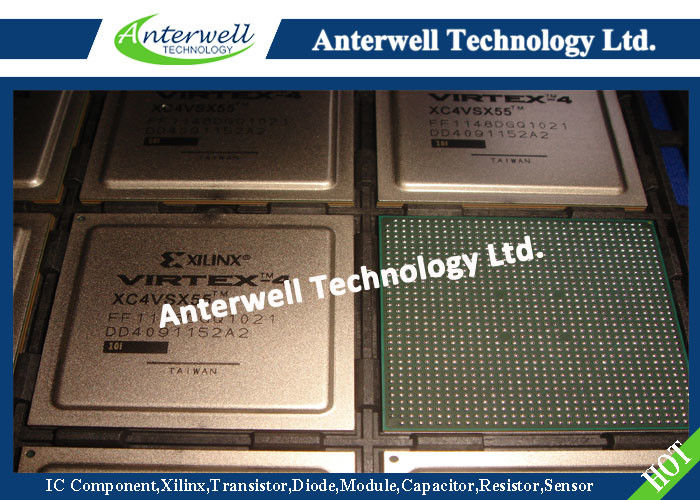
XC4VSX55- FF1148DGQ1021 Programmable IC Chips , integrated programmed
Stock Offer (Hot Sell)
| Part no. | Quantity | Brand | D/C | Package |
| 74HC147D | 2500 | ST | 15+ | SOP-16 |
| 74HC151 | 2500 | NXP | 16+ | SOP |
| 74HC4066PW | 2500 | NXP | 16+ | TSSOP |
| 74HC4538D | 2500 | NXP | 14+ | SOP-16 |
| 74LCX74MTCX | 2500 | FAIRCHILD | 14+ | TSSOP |
| 74LVC08AD | 2500 | PHI | 14+ | SOP14 |
| AMS1117-5.0V | 2500 | AMS | 16+ | SOT-223 |
| ATMEGA162-16PU | 2500 | ATMEL | 16+ | DIP-40 |
| BC817-40 | 2500 | NXP | 13+ | SOT-23 |
| BTB16-800CW | 2500 | ST | 15+ | TO-220 |
| CC2541F256RHAR | 2500 | TI | 16+ | VQFN40 |
| CD4052 | 2500 | TI | 16+ | DIPSOP |
| FQP50N06 | 2500 | FAIRCHILD | 14+ | TO-220 |
| HD74LS161 | 2500 | HIT | 14+ | DIP |
| HEF4011 | 2500 | NXP | 14+ | DIP |
| HEF4011BT | 2500 | NXP | 16+ | SO-14 |
| IRF7416TRPBF | 2500 | IR | 16+ | SOP-8 |
| KSZ8721BL | 2500 | MICREL | 13+ | QFP |
| LM3102MHX | 2500 | NS | 15+ | TSSOP-20 |
| LM78L05ACMX | 2500 | NS | 16+ | SOP-8 |
| LTC1688CS#PBF | 2500 | LINEAR | 16+ | SOP-16 |
| MAX4252EUA | 2500 | MAXIM | 14+ | MSOP8 |
| MAX6315US26D1 | 2500 | MAXIM | 14+ | SOT143 |
| MC908JL3ECPE | 2500 | FREESCALE | 14+ | DIP28 |
| MCP2551T-I/SN | 2500 | MICROCHIP | 16+ | SOP8 |
| MJD44H11 | 2500 | ON | 16+ | TO-252 |
| MPQ2222A | 2500 | MOT | 13+ | DIP |
| MX25L12805DMI-20G | 2500 | MXIC | 15+ | SOP16 |
| NCP1200D60R2G | 2500 | ON | 16+ | SOP-8 |
| NSS40301MZ4T1G | 2500 | ON | 16+ | SOT223 |
Virtex-4 FPGA Data Sheet: DC and Switching Characteristics
Virtex-4 FPGA Electrical Characteristics
Virtex®-4 FPGAs are available in -12, -11, and -10 speed grades, with -12 having the highest performance.
Virtex-4 FPGA DC and AC characteristics are specified for both commercial and industrial grades. Except the operating temperature range or unless otherwise noted, all the DC and AC electrical parameters are the same for a particular speed grade (that is, the timing characteristics of a -10 speed grade industrial device are the same as for a -10 speed grade commercial device). However, only selected speed grades and/or devices might be available in the industrial range.
All supply voltage and junction temperature specifications are representative of worst-case conditions. The parameters included are common to popular designs and typical applications.
This Virtex-4 FPGA Data Sheet is part of an overall set of documentation on the Virtex-4 family of FPGAs that is available on the Xilinx website:
• Virtex-4 Family Overview, DS112
• Virtex-4 FPGA User Guide, UG070
• Virtex-4 Configuration Guide, UG071
• XtremeDSP for Virtex-4 FPGAs User Guide, UG073
• Virtex-4 Packaging and Pinout Specification, UG075
• Virtex-4 PCB Designer’s Guide, UG072
• Virtex-4 RocketIO™ Multi-Gigabit Transceiver User Guide, UG076
• Virtex-4 FPGA Embedded Tri-Mode Ethernet MAC User Guide, UG074
• PowerPC® 405 Processor Block Reference Guide, UG018
All specifications are subject to change without notice.
Absolute Maximum Ratings
| Symbol | Description | Units | |
| VCCINT | Internal supply voltage relative to GND | –0.5 to 1.32 | V |
| VCCAUX | Auxiliary supply voltage relative to GND | –0.5 to 3.0 | V |
| VCCO | Output drivers supply voltage relative to GND | –0.5 to 3.75 | V |
| VBATT | Key memory battery backup supply | –0.5 to 4.05 | V |
| VREF | Input reference voltage | –0.3 to 3.75 | V |
| VIN | I/O input voltage relative to GND (all user and dedicated I/Os) | –0.75 to 4.05 | V |
| I/O input voltage relative to GND (restricted to maximum of 100 user I/Os)(3,4) |
–0.95 to 4.4 (Commercial Temperature) –0.85 to 4.3 (Industrial Temperature) |
V | |
| 2.5V or below I/O input voltage relative to GND (user and dedicated I/Os) | –0.75 to VCCO +0.5 | V | |
| IIN | Current applied to an I/O pin, powered or unpowered | ±100 | mA |
| Total current applied to all I/O pins, powered or unpowered | ±200 | mA | |
| VTS | Voltage applied to 3-state 3.3V output (all user and dedicated I/Os) | –0.75 to 4.05 | V |
| Voltage applied to 3-state 3.3V output (restricted to maximum of 100 user I/Os)(3,4) |
–0.95 to 4.4 (Commercial Temperature) –0.85 to 4.3 (Industrial Temperature) |
V | |
| 2.5V or below I/O input voltage relative to GND (user and dedicated I/Os) | –0.75 to VCCO +0.5 | V | |
| AVCCAUXRX | Receive auxiliary supply voltage relative to analog ground, GNDA (RocketIO pins) | –0.5 to 1.32 | V |
| AVCCAUXTX | Transmit auxiliary supply voltage relative to analog ground, GNDA (RocketIO pins) | –0.5 to 1.32 | V |
| AVCCAUXMGT | Management auxiliary supply voltage relative to analog ground, GNDA (RocketIO pins) | –0.5 to 3.0 | V |
| VTRX | Terminal receive supply voltage relative to GND | –0.5 to 3.0 | V |
| VTTX | Terminal transmit supply voltage relative to GND | –0.5 to 1.65 | V |
| TSTG | Storage temperature (ambient) | –65 to 150 | ° C |
| TSOL | Maximum soldering temperature(2) | +220 | ° C |
| TJ | Maximum junction temperature(2) | +125 | ° C |
Notes:
1. Stresses beyond those listed under Absolute Maximum Ratings might cause permanent damage to the device. These are stress ratings only, and functional operation of the device at these or any other conditions beyond those listed under Operating Conditions is not implied. Exposure to Absolute Maximum Ratings conditions for extended periods of time might affect device reliability.
2. For soldering guidelines and thermal considerations, see the Virtex-4 Packaging and Pinout Specification on the Xilinx website.
3. When using more than 100 3.3V I/Os, refer to the Virtex-4 FPGA User Guide, Chapter 6, “3.3V I/O Design Guidelines.”
4. For more flexibility in specific designs, a maximum of 100 user I/Os can be stressed beyond the normal spec for no more than 20% of a data period. There are no bank restrictions.
High Power Rectifier Diode 1N4756A , Silicon Planar Zener Diodes
Bridge Type Rectifier Diode 1N4007 50 to 1000 Volts 1.0 Ampere
1N4742A Silicon Planar Zener Diodes for Stabilized Power Supply
Power Programmable IC Chips XC6SLX100-3FGG484C Spartan-6 Family Overview
128K Bytes Sound IC Chip Programming ATMEGA128-16AU 8 Bit Microcontroller
EMC Programmable IC Chips Compliant Slew Rate Limited EI , Timer IC Chip
SMD Power Mosfet Module L7812CV TO-220 Power Trans Electronic Compoents
2SD1594 3 Pin Transistor NEC NPN Power Transistor Switching High Speed
2N5459 Power Mosfet Transistor N-Channel To-92 Original Stock FSC