Anterwell Technology Ltd.
Anterwell Technology Ltd.
Large Original stock of IC Electronics Components, Transistors, Diodes etc.
High Quality, Reasonable Price, Fast Delivery.
Anterwell Technology Ltd.
Large Original stock of IC Electronics Components, Transistors, Diodes etc.
High Quality, Reasonable Price, Fast Delivery.


Product Details:
Payment & Shipping Terms:
|
| Supply Voltage: | 7 V | Input Voltage: | ±25 V |
|---|---|---|---|
| Differential Input Voltage: | ±25 V | Low-level Output Current: | 50 MA |
| Case Temperature For 60 Seconds: | 260 °C | Storage Temperature Range: | –65°C To 150°C |
| Highlight: | electronics ic chip,integrated circuit components |
||
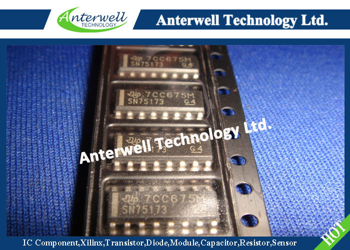
SN75173 Linear Integrated Circuits Quadruple Differential Line Receivers
SN55173, SN65173, SN75173
QUADRUPLE DIFFERENTIAL LINE RECEIVERS
description
The SN55173, SN65173, and SN75173 are monolithic quadruple differential line receivers with 3-state outputs. They are designed to meet the requirements of TIA/EIA-422-B, TIA/EIA-423-B, TIA/EIA-485-A, and several ITU recommendations. The standards are for balanced multipoint bus transmission at rates up to 10 megabits per second. The four receivers share two OR enable inputs, one active when high, the other active when low. These devices feature high input impedance, input hysteresis for increased noise immunity, and input sensitivity of ±200 mV over a common-mode input voltage range of –12 V to 12 V. Fail-safe design specifies that if the inputs are open circuited, the outputs are always high. The SN65173 and SN75173 are designed for optimum performance when used with the SN75172 or SN75174 quad differential line drivers.
The SN55173 is characterized over the full military temperature range of –55°C to 125°C. The SN65173 is characterized for operation from –40°C to 85°C. The SN75173 is characterized for operation from 0°C to 70°C.
absolute maximum ratings over operating free-air temperature range
(unless otherwise noted)†
Supply voltage, VCC (see Note 1) . . . . . . . . . . . . . . . . . . . . . . . . . . . . . . . . . . . . . . . . . . . . . . . . 7 V
Input voltage (VI or B inputs) . . . . . . . . . . . . . . . . . . . . . . . . . . . . . . . . . . . . . . . . . . . . . . . . . . . . ±25 V
Differential input voltage, VID (see Note 2) . . . . . . . . . . . . . . . . . . . . . . . . . . . . . . . . . . . . . . . . . ±25 V
Enable input voltage, VI . . . . . . . . . . . . . . . . . . . . . . . . . . . . . . . . . . . . . . . . . . . . . . . . . . . . . . . . . . 7 V
Low-level output current, IOL . . . . . . . . . . . . . . . . . . . . . . . . . . . . . . . . . . . . . . . . . . . . . . . . . . . 50 mA
Package thermal impedance, θJA (see Note 3): D package .. . . . . . . . . . . . . . . . . . . . . . . . . . 73 °C/W
N package . . . . . . . . . . . .. . . . . . . . . . . . . . . 67 °C/W
Continuous total dissipation . . . . . . . . . . . . . . . . . . . . . . . . . . . . . . . . . . . See Dissipation Rating Table
Case temperature for 60 seconds, TC: FK package . . . . . . . . . . . . . . . . . . . . . . . . . . . . . . . . . . 260°C
Lead temperature 1,6 mm (1/16 inch) from case for 10 seconds: D or N package . . . . . . . . . . . 260°C
Lead temperature 1,6 mm (1/16 inch) from case for 60 seconds: J package . . . . . . . . . . . . . . . 300°C
Storage temperature range, Tstg . . . . . . . . . . . . . . . . . . . . . . . . . . . . . . . . . . . . . . . . . –65°C to 150°C
† Stresses beyond those listed under “absolute maximum ratings” may cause permanent damage to the device. These are stress ratings only, and functional operation of the device at these or any other conditions beyond those indicated under “recommended operating conditions” is not implied. Exposure to absolute-maximum-rated conditions for extended periods may affect device reliability.
NOTES:
1. All voltage values, except differential input voltage, are with respect to network ground terminal.
2. Differential input voltage is measured at the noninverting input with respect to the corresponding inverting input.
3. The package thermal impedance is calculated in accordance with JESD 51.
THE SN55173 IS NOT RECOMMENDED FOR NEW DESIGNS.
![]()
![]()
logic symbol †
![]()
logic diagram (positive logic)
![]()
schematics of inputs and outputs
![]()
High Power Rectifier Diode 1N4756A , Silicon Planar Zener Diodes
Bridge Type Rectifier Diode 1N4007 50 to 1000 Volts 1.0 Ampere
1N4742A Silicon Planar Zener Diodes for Stabilized Power Supply
Power Programmable IC Chips XC6SLX100-3FGG484C Spartan-6 Family Overview
128K Bytes Sound IC Chip Programming ATMEGA128-16AU 8 Bit Microcontroller
EMC Programmable IC Chips Compliant Slew Rate Limited EI , Timer IC Chip
SMD Power Mosfet Module L7812CV TO-220 Power Trans Electronic Compoents
2SD1594 3 Pin Transistor NEC NPN Power Transistor Switching High Speed
2N5459 Power Mosfet Transistor N-Channel To-92 Original Stock FSC