Anterwell Technology Ltd.
Anterwell Technology Ltd.
Large Original stock of IC Electronics Components, Transistors, Diodes etc.
High Quality, Reasonable Price, Fast Delivery.
Anterwell Technology Ltd.
Large Original stock of IC Electronics Components, Transistors, Diodes etc.
High Quality, Reasonable Price, Fast Delivery.


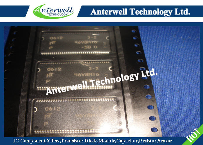
Product Details:
Payment & Shipping Terms:
|
| VDD: | +2.5V ±0.2V | VDDQ: | +2.5V ±0.2V |
|---|---|---|---|
| I/O: | 2.5V | Package: | FBGA Package Available |
| Clock: | 167 MHz | Data Rate: | 333 Mb/s/p |
| High Light: | integrated circuit ic,integrated circuit components |
||
DOUBLE DATA RATE (DDR) SDRAM
FEATURES
• 167 MHz Clock, 333 Mb/s/p data rate
• VDD = +2.5V ±0.2V, VDDQ = +2.5V ±0.2V
• Bidirectional data strobe (DQS) transmitted/ received with data, i.e., source-synchronous data capture (x16 has two - one per byte)
• Internal, pipelined double-data-rate (DDR) architecture; two data accesses per clock cycle
• Differential clock inputs (CK and CK#)
• Commands entered on each positive CK edge
• DQS edge-aligned with data for READs; centeraligned with data for WRITEs
• DLL to align DQ and DQS transitions with CK
• Four internal banks for concurrent operation
• Data mask (DM) for masking write data (x16 has two - one per byte)
• Programmable burst lengths: 2, 4, or 8
• Concurrent Auto Precharge option supported
• Auto Refresh and Self Refresh Modes
• FBGA package available
• 2.5V I/O (SSTL_2 compatible)
• t RAS lockout (t RAP = t RCD)
• Backwards compatible with DDR200 and DDR266
OPTIONS PART NUMBER
• Configuration
32 Meg x 4 (8 Meg x 4 x 4 banks) 32M4
16 Meg x 8 (4 Meg x 8 x 4 banks) 16M8
8 Meg x 16 (2 Meg x 16 x 4 banks) 8M16
• Plastic Package
66-Pin TSOP (OCPL) TG
60-Ball FBGA (16x9mm) FJ
• Timing - Cycle Time
6ns @ CL = 2.5 (DDR333B–FBGA)1 -6
6ns @ CL = 2.5 (DDR333B–TSOP)1 -6T
7.5ns @ CL = 2 (DDR266A)2 -75Z
• Self Refresh
Standard none
NOTE: 1. Supports PC2700 modules with 2.5-3-3 timing
2. Supports PC2100 modules with 2-3-3 timing
DDR333 COMPATIBILITY
DDR333 meets or surpasses all DDR266 timing requirements thus assuring full backwards compatibility with current DDR designs. In addition, these devices support concurrent auto-precharge and t RAS lockout for improved timing performance. The 128Mb, DDR333 device will support an (t REFI) average periodic refresh interval of 15.6µs.
The standard 66-pin TSOP package is offered for point-to-point applications where the FBGA package is intended for the multi-drop systems.
The Micron 128Mb data sheet provides full specifications and functionality unless specified herein.
FBGA 60-BALL PACKAGE DIMENSION
![]()
FBGA PACKAGE MARKING
Due to the physical size of the FBGA package, the full ordering part number is not printed on the package. Instead the following package code is utilized.
Top mark contains five fields 12345
• Field 1 (Product Family)
DRAM D
DRAM - ES Z
• Field 2 (Product Type)
2.5 Volt, DDR SDRAM, 60-ball L
• Field 3 (Width)
x4 devices B
x8 devices C
x16 devices D
• Field 4 (Density / Size)
128Mb F
• Filed 5 (Speed Grade)
-6 J
-75Z P
-75 F
-8 C
66-PIN TSOP PACKAGE DIMENSION 66-PIN TSOP PACKAGE PIN ASSIGMENT
![]()
High Power Rectifier Diode 1N4756A , Silicon Planar Zener Diodes
Bridge Type Rectifier Diode 1N4007 50 to 1000 Volts 1.0 Ampere
1N4742A Silicon Planar Zener Diodes for Stabilized Power Supply
Power Programmable IC Chips XC6SLX100-3FGG484C Spartan-6 Family Overview
128K Bytes Sound IC Chip Programming ATMEGA128-16AU 8 Bit Microcontroller
EMC Programmable IC Chips Compliant Slew Rate Limited EI , Timer IC Chip
SMD Power Mosfet Module L7812CV TO-220 Power Trans Electronic Compoents
2SD1594 3 Pin Transistor NEC NPN Power Transistor Switching High Speed
2N5459 Power Mosfet Transistor N-Channel To-92 Original Stock FSC