Anterwell Technology Ltd.
Anterwell Technology Ltd.
Large Original stock of IC Electronics Components, Transistors, Diodes etc.
High Quality, Reasonable Price, Fast Delivery.
Anterwell Technology Ltd.
Large Original stock of IC Electronics Components, Transistors, Diodes etc.
High Quality, Reasonable Price, Fast Delivery.


Product Details:
Payment & Shipping Terms:
|
| Supply Voltage Range: | –0.3 V To 6 V | Positive Output Supply Voltage Range, V+: | –0.3 V To 7 V |
|---|---|---|---|
| Negative Output Supply Voltage Range, V–: | 0.3 V To –7 V | Supply Voltage Difference, V+ – V–: | 13 V |
| Lead Temperature 1,6 Mm (1/16 Inch) From Case For 10 Seconds: | 260 °C | Storage Temperature Range: | –65°C To 150°C |
| Highlight: | integrated circuit ic,integrated circuit components |
||
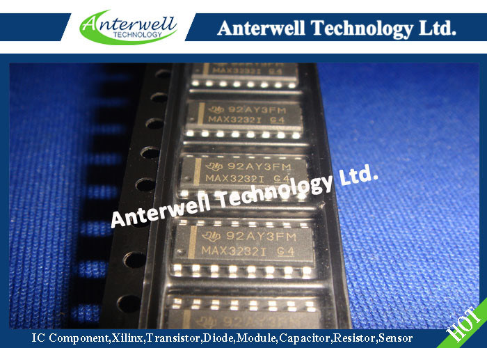
MAX3232
3-V TO 5.5-V MULTICHANNEL RS-232 LINE DRIVER/RECEIVER
description
The MAX3232 device consists of two line drivers, two line receivers, and a dual charge-pump circuit with ±15-kV ESD protection pin to pin (serial-port connection pins, including GND). The device meets the requirements of TIA/EIA-232-F and provides the electrical interface between an asynchronous communication controller and the serial-port connector. The charge pump and four small external capacitors allow operation from a single 3-V to 5.5-V supply. The devices operate at data signaling rates up to 250 kbit/s and a maximum of 30-V/µs driver output slew rate.
The MAX3232C is characterized for operation from 0°C to 70°C. The MAX3232I is characterized for operation from –40°C to 85°C.
absolute maximum ratings over operating free-air temperature range
(unless otherwise noted)†
Supply voltage range, VCC (see Note 1) . . . . . . . . . . . . . . . . . . . . . . . . . . . . . . . . . . . . . . –0.3 V to 6 V
Positive output supply voltage range, V+ (see Note 1) . . . . . . . . . .. . . . . . . . . . . . . . . . . . –0.3 V to 7 V
Negative output supply voltage range, V– (see Note 1) . . . . . . . . . . . . . . . . . . . . . . . . . . .0.3 V to –7 V
Supply voltage difference, V+ – V– (see Note 1) . . . . . . . . . . . . . . . . . . . . . . . . . . . . . . . . . . . . . . 13 V
Input voltage range, VI : Drivers . . . . . . . . . . . . . . . . . . . . . . . . . . . . . . . . . . . . . . . . . . . . –0.3 V to 6 V
Receivers . . . . . . . . . . . . . . . . . . . . . . . . . . . . . . . . . . . . . . . . .. . –25 V to 25 V
Output voltage range, VO: Drivers . . . . . . . . . . . . . . . . . . . . . . . . . . . . . . . . . . . . . . . . –13.2 V to 13.2 V
Receivers . . . . . . . . . . . . . . . . . . . . . . . . . . . . . . . . . . –0.3 V to VCC + 0.3 V
Package thermal impedance, θJA (see Note 2): D package . . . . . . . . . . . . . . . . . . . . . . . . . . . .73°C/W
DB package . . . . . . . . . . . . . . . . . . . . . . . . . . . 82°C/W
DW package . . . . . . . . . . . . . . . . . . . . . . . . . . . .57°C/W
PW package . . . . . . . . . . . . . . . . . . . . . . . . . . .108°C/W
Lead temperature 1,6 mm (1/16 inch) from case for 10 seconds . . . . . .. . . . . . . . . . . . . . . . . . . . 260°C
Storage temperature range, Tstg . . . . . . . . . . . . . . . . . . . . . . . . . . . . . . . . . . . . . . . . . . –65°C to 150°C
† Stresses beyond those listed under “absolute maximum ratings” may cause permanent damage to the device. These are stress ratings only, and functional operation of the device at these or any other conditions beyond those indicated under “recommended operating conditions” is not implied. Exposure to absolute-maximum-rated conditions for extended periods may affect device reliability.
NOTES: 1. All voltages are with respect to network GND.
2. The package thermal impedance is calculated in accordance with JESD 51-7.
D, DB, DW, OR PW PACKAGE (TOP VIEW)
![]()
logic diagram (positive logic)
![]()
APPLICATION INFORMATION
![]()
High Power Rectifier Diode 1N4756A , Silicon Planar Zener Diodes
Bridge Type Rectifier Diode 1N4007 50 to 1000 Volts 1.0 Ampere
1N4742A Silicon Planar Zener Diodes for Stabilized Power Supply
Power Programmable IC Chips XC6SLX100-3FGG484C Spartan-6 Family Overview
128K Bytes Sound IC Chip Programming ATMEGA128-16AU 8 Bit Microcontroller
EMC Programmable IC Chips Compliant Slew Rate Limited EI , Timer IC Chip
SMD Power Mosfet Module L7812CV TO-220 Power Trans Electronic Compoents
2SD1594 3 Pin Transistor NEC NPN Power Transistor Switching High Speed
2N5459 Power Mosfet Transistor N-Channel To-92 Original Stock FSC