Anterwell Technology Ltd.
Anterwell Technology Ltd.
Large Original stock of IC Electronics Components, Transistors, Diodes etc.
High Quality, Reasonable Price, Fast Delivery.
Anterwell Technology Ltd.
Large Original stock of IC Electronics Components, Transistors, Diodes etc.
High Quality, Reasonable Price, Fast Delivery.


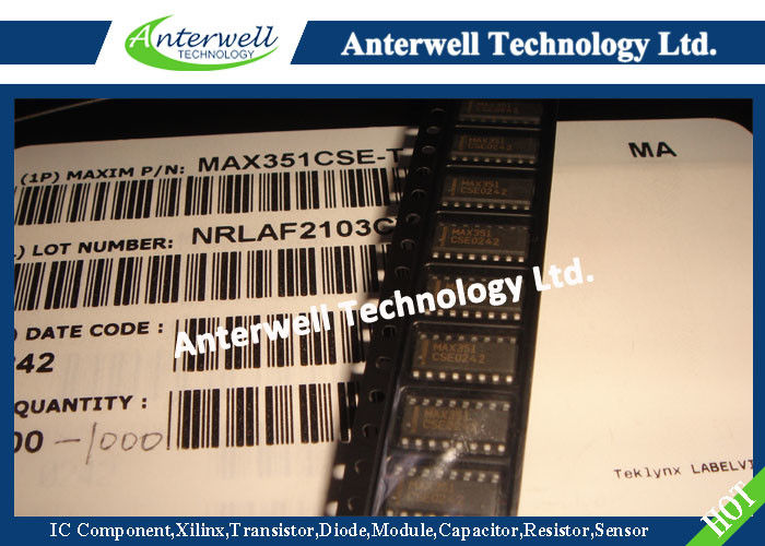
Product Details:
Payment & Shipping Terms:
|
| Input Current With Input Voltage High: | 0.005 µA | Input Current With Input Voltage Low: | 0.005 µA |
|---|---|---|---|
| Power-Supply Range: | ±4.5 To ±20.0 V | On Capacitance: | 35 PF |
| Storage Temperature Range: | -65°C To +150°C | Lead Temperature (soldering, 10sec): | +300°C |
| Highlight: | electronics ic chip,integrated circuit ic |
||
Precision, Quad, SPST Analog Switches
General Description
The MAX351/MAX352/MAX353 are precision, quad, single-pole single-throw (SPST) analog switches. The MAX351 has four normally closed (NC), and the MAX352 has four normally open (NO) switches. The MAX353 has two NO and two NC switches. All three parts offer low on resistance (less than 35Ω), guaranteed to match within 2Ω between channels and to remain flat over the analog signal range (∆3Ω max). They also offer low leakage (less than 250pA at +25°C and less than 6nA at +85°C) and fast switching (turn-on time less than 175ns and turn-off time less than 145ns).
The MAX351/MAX352/MAX353 are fabricated with Maxim’s new improved 44V silicon-gate process. Design improvements guarantee extremely low charge injection (10pC), low power consumption (35µW), and electrostatic discharge (ESD) greater than 2000V. The 44V maximum breakdown voltage allows rail-to-rail analog signal handling.
These monolithic switches operate with a single positive supply (+10V to +30V) or with split supplies (±4.5V to ±20V) while retaining CMOS-logic input compatibility and fast switching. CMOS inputs provide reduced input loading.
Applications
Sample-and-Hold Circuits Military Radios
Guidance and Control Systems Communications Systems
Heads-Up Displays Battery-Operated Systems
Test Equipment PBX, PABX
Features
♦ Low On Resistance < 22Ω Typical (35Ω Max)
♦ Guaranteed Matched On Resistance Between Channels < 2Ω
♦ Guaranteed Flat On Resistance Over Analog Signal Range ∆3Ω Max
♦ Guaranteed Charge Injection < 10pC
♦ Guaranteed Off-Channel Leakage < 6nA at +85°C
♦ ESD Guaranteed > 2000V per Method 3015.7
♦ Single-Supply Operation (+10V to +30V) Bipolar-Supply Operation (±4.5V to ±20V)
♦ TTL-/CMOS-Logic Compatibility
♦ Rail-to-Rail Analog Signal Handling Capability
ABSOLUTE MAXIMUM RATINGS
Voltage Referenced to V-
V+.......................................................................................44V
GND ...................................................................................25V
VL ................................................(GND - 0.3V) to (V+ + 0.3V)
Digital Inputs, VCOM, VNC, VNO (Note 1)...........(V- - 2V) to (V+ + 2V)
.........................................................or 30mA(whichever occurs first)
Current (any terminal) .........................................................30mA
Peak Current COM_, NO_, NC_
(pulsed at 1ms, 10% duty cycle max) ..........................100mA
ESD per Method 3015.7 ..................................................>2000V
Continuous Power Dissipation (TA = +70°C) (Note 2)
Plastic DIP (derate 10.53mW/°C above +70°C) ..........842mW
Narrow SO (derate 8.70mW/°C above +70°C) ............696mW
CERDIP (derate 10.00mW/°C above +70°C)...............800mW
Operating Temperature Ranges:
MAX35_C_ _ .......................................................0°C to +70°C
MAX35_E_ _.....................................................-40°C to +85°C
MAX35_MJE ..................................................-55°C to +125°C
Storage Temperature Range .............................-65°C to +150°C
Lead Temperature (soldering, 10sec) .............................+300°C
Note 1: Signals on NC_, NO_, COM_, or IN_ exceeding V+ or V- will be clamped by internal diodes. Limit forward diode current to maximum current rating.
Note 2: All leads are soldered or welded to PC board.
Stresses beyond those listed under “Absolute Maximum Ratings” may cause permanent damage to the device. These are stress ratings only, and functional operation of the device at these or any other conditions beyond those indicated in the operational sections of the specifications is not implied. Exposure to absolute maximum rating conditions for extended periods may affect device reliability.
Pin Configurations/Functional Diagrams/Truth Tables
![]()
High Power Rectifier Diode 1N4756A , Silicon Planar Zener Diodes
Bridge Type Rectifier Diode 1N4007 50 to 1000 Volts 1.0 Ampere
1N4742A Silicon Planar Zener Diodes for Stabilized Power Supply
Power Programmable IC Chips XC6SLX100-3FGG484C Spartan-6 Family Overview
128K Bytes Sound IC Chip Programming ATMEGA128-16AU 8 Bit Microcontroller
EMC Programmable IC Chips Compliant Slew Rate Limited EI , Timer IC Chip
SMD Power Mosfet Module L7812CV TO-220 Power Trans Electronic Compoents
2SD1594 3 Pin Transistor NEC NPN Power Transistor Switching High Speed
2N5459 Power Mosfet Transistor N-Channel To-92 Original Stock FSC