Anterwell Technology Ltd.
Anterwell Technology Ltd.
Large Original stock of IC Electronics Components, Transistors, Diodes etc.
High Quality, Reasonable Price, Fast Delivery.
Anterwell Technology Ltd.
Large Original stock of IC Electronics Components, Transistors, Diodes etc.
High Quality, Reasonable Price, Fast Delivery.


Product Details:
Payment & Shipping Terms:
|
| AVDD To AGND: | −0.3 V To +2.0 V | D0 Through D13 To DGND: | −0.3 V To DRVDD + 0.3 V |
|---|---|---|---|
| Storage Temperature Range: | –65°C To +125°C | Operating Temperature Range: | –40°C To +85°C |
| Lead Temperature (Soldering 10 Sec): | +300°C | Junction Temperature: | +150°C |
| Highlight: | programming ic chips,ic programmer circuit |
||
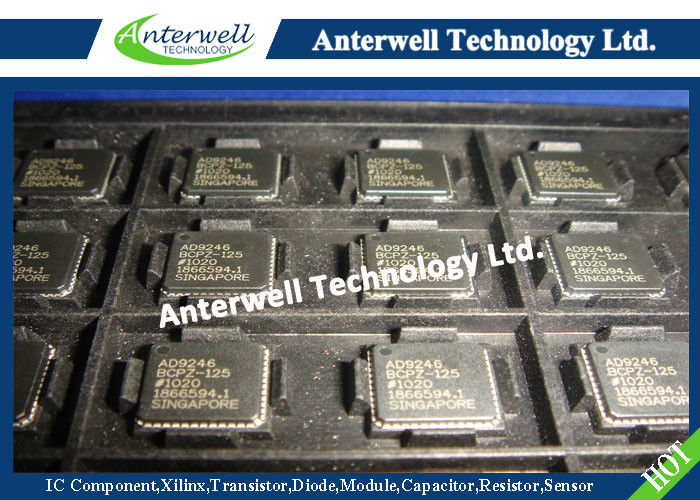
14-Bit, 80 MSPS/105 MSPS/125 MSPS, 1.8 V Analog-to-Digital Converter AD9246
FEATURES
1.8 V analog supply operation
1.8 V to 3.3 V output supply
SNR = 71.7 dBc (72.7 dBFS) to 70 MHz input
SFDR = 85 dBc to 70 MHz input
Low power: 395 mW @ 125 MSPS
Differential input with 650 MHz bandwidth
On-chip voltage reference and sample-and-hold amplifier
DNL = ±0.4 LSB
Flexible analog input: 1 V p-p to 2 V p-p range
Offset binary, Gray code, or twos complement data format
Clock duty cycle stabilizer
Data output clock
Serial port control
Built-in selectable digital test pattern generation
Programmable clock and data alignment
APPLICATIONS
Ultrasound equipment
IF sampling in communications receivers
IS-95, CDMA-One, IMT-2000
Battery-powered instruments
Hand-held scopemeters
Low cost digital oscilloscopes
GENERAL DESCRIPTION
The AD9246 is a monolithic, single 1.8 V supply, 14-bit, 80 MSPS/ 105 MSPS/125 MSPS analog-to-digital converter (ADC), featuring a high performance sample-and-hold amplifier (SHA) and on-chip voltage reference. The product uses a multistage differential pipeline architecture with output error correction logic to provide 14-bit accuracy at 125 MSPS data rates and guarantees no missing codes over the full operating temperature range.
The wide bandwidth, truly differential SHA allows a variety of user-selectable input ranges and offsets, including single-ended applications. It is suitable for multiplexed systems that switch full-scale voltage levels in successive channels and for sampling single-channel inputs at frequencies well beyond the Nyquist rate. Combined with power and cost savings over previously available ADCs, the AD9246 is suitable for applications in communications, imaging, and medical ultrasound.
A differential clock input controls all internal conversion cycles. A duty cycle stabilizer (DCS) compensates for wide variations in the clock duty cycle while maintaining excellent overall ADC performance.
The digital output data is presented in offset binary, Gray code, or twos complement formats. A data output clock (DCO) is provided to ensure proper latch timing with receiving logic.
The AD9246 is available in a 48-lead LFCSP_VQ and is specified over the industrial temperature range (−40°C to +85°C).
PRODUCT HIGHLIGHTS
1. The AD9246 operates from a single 1.8 V power supply and features a separate digital output driver supply to accommodate 1.8 V to 3.3 V logic families.
2. The patented SHA input maintains excellent performance for input frequencies up to 225 MHz.
3. The clock DCS maintains overall ADC performance over a wide range of clock pulse widths.
4. A standard serial port interface supports various product features and functions, such as data formatting (offset binary, twos complement, or Gray coding), enabling the clock DCS, power-down, and voltage reference mode.
5. The AD9246 is pin-compatible with the AD9233, allowing a simple migration from 12 bits to 14 bits.
ABSOLUTE MAXIMUM RATINGS
| Parameter | Rating |
| ELECTRICAL | |
| AVDD to AGND | −0.3 V to +2.0 V |
| DRVDD to DGND | −0.3 V to +3.9 V |
| AGND to DGND | −0.3 V to +0.3 V |
| AVDD to DRVDD | −3.9 V to +2.0 V |
| D0 through D13 to DGND | −0.3 V to DRVDD + 0.3 V |
| DCO to DGND | −0.3 V to DRVDD + 0.3 V |
| OR to DGND | −0.3 V to DRVDD + 0.3 V |
| CLK+ to AGND | −0.3 V to +3.9 V |
| CLK− to AGND | −0.3 V to +3.9 V |
| VIN+ to AGND | −0.3 V to AVDD + 0.2 V |
| VIN− to AGND | −0.3 V to AVDD + 0.2 V |
| VREF to AGND | −0.3 V to AVDD + 0.2 V |
| SENSE to AGND | −0.3 V to AVDD + 0.2 V |
| REFT to AGND | −0.3 V to AVDD + 0.2 V |
| REFB to AGND | −0.3 V to AVDD + 0.2 V |
| SDIO/DCS to DGND | −0.3 V to DRVDD + 0.3 V |
| PDWN to AGND | −0.3 V to +3.9 V |
| CSB to AGND | −0.3 V to +3.9 V |
| SCLK/DFS to AGND | −0.3 V to +3.9 V |
| OEB to AGND | −0.3 V to +3.9 V |
| ENVIRONMENTAL | |
| Storage Temperature Range | –65°C to +125°C |
| Operating Temperature Range | –40°C to +85°C |
| Lead Temperature (Soldering 10 Sec) | +300°C |
| Junction Temperature | +150°C |
Stresses above those listed under Absolute Maximum Ratings may cause permanent damage to the device. This is a stress rating only; functional operation of the device at these or any other conditions above those indicated in the operational section of this specification is not implied. Exposure to absolute maximum rating conditions for extended periods may affect device reliability.
FUNCTIONAL BLOCK DIAGRAM
![]()
OUTLINE DIMENSIONS
![]()
Stock Offer (Hot Sell)
| Part NO. | Q'ty | MFG | D/C | Package |
| LTM8052EV#PBF | 1817 | LINEAR | 16+ | LGA |
| MPZ1005S121CT000 | 20000 | TDK | 16+ | SMD |
| PE42551 | 14240 | PEREGRINE | 16+ | QFN |
| PBSS5320T | 40000 | NXP | 16+ | SOT-23 |
| LT3508EFE#PBF | 3118 | LINEAR | 16+ | TSSOP |
| NR6020T4R7N | 10000 | TAIYO | 16+ | SMD |
| PMBTA45 | 18000 | NXP | 14+ | SOT-23 |
| PIC18F452-I/P | 4453 | MICROCHIP | 15+ | TQFP |
| PIC18F25K80-I/MM | 4533 | MICROCHIP | 13+ | QFN |
| MIC2026-1YMTR | 6364 | MICREL | 16+ | SOP |
| MT29F4G08ABADAH4-IT:D | 6974 | MICRON | 14+ | FBGA |
| MBR140SFT1G | 25000 | ON | 16+ | SOD |
| MCP2200-I/SO | 5146 | MICROCHIP | 16+ | SOP |
| LM555CH | 1345 | NSC | 15+ | CAN-8 |
| PIC18LF6621-I/PT | 4203 | MICROCHIP | 15+ | QFP |
| LMH6645MAX | 634 | NSC | 15+ | SOP-8 |
| N28F010-150 | 4480 | INTEL | 10+ | PLCC |
| MCP6001T-E/LT | 5386 | MICROCHIP | 16+ | SC70-5 |
| LM324AN | 5000 | TI | 11+ | DIP-14 |
| LT1129CST-5.0 | 8674 | LT | 16+ | SOT-223 |
| NRF24L01P(P+1 is same) | 3880 | NORDIC | 16+ | QFN |
High Power Rectifier Diode 1N4756A , Silicon Planar Zener Diodes
Bridge Type Rectifier Diode 1N4007 50 to 1000 Volts 1.0 Ampere
1N4742A Silicon Planar Zener Diodes for Stabilized Power Supply
Power Programmable IC Chips XC6SLX100-3FGG484C Spartan-6 Family Overview
128K Bytes Sound IC Chip Programming ATMEGA128-16AU 8 Bit Microcontroller
EMC Programmable IC Chips Compliant Slew Rate Limited EI , Timer IC Chip
SMD Power Mosfet Module L7812CV TO-220 Power Trans Electronic Compoents
2SD1594 3 Pin Transistor NEC NPN Power Transistor Switching High Speed
2N5459 Power Mosfet Transistor N-Channel To-92 Original Stock FSC