Anterwell Technology Ltd.
Anterwell Technology Ltd.
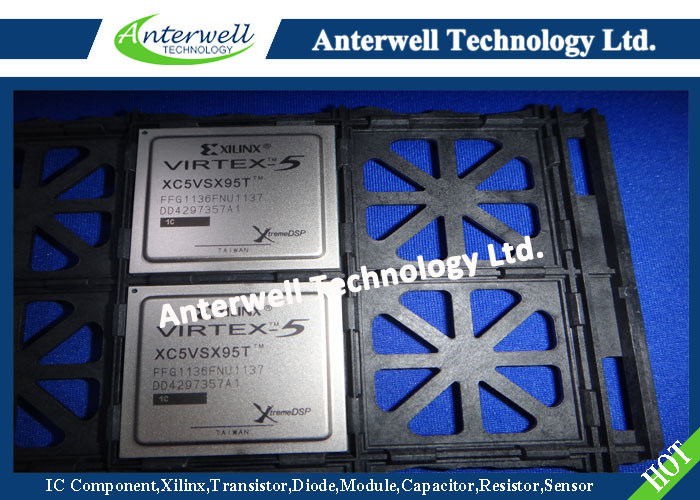
Large Original stock of IC Electronics Components, Transistors, Diodes etc.
High Quality, Reasonable Price, Fast Delivery.
Anterwell Technology Ltd.
Large Original stock of IC Electronics Components, Transistors, Diodes etc.
High Quality, Reasonable Price, Fast Delivery.


|
Product Details:
Payment & Shipping Terms:
|
| Virtex-5 LX: | High-performance General Logic Applications | Virtex-5 LXT: | High-performance Logic With Advanced Serial Connectivity |
|---|---|---|---|
| Virtex-5 SXT: | High-performance Signal Processing Applications With Advanced Serial Connectivity | Virtex-5 TXT: | High-performance Systems With Double Density Advanced Serial Connectivity |
| Virtex-5 FXT: | High-performance Embedded Systems With Advanced Serial Connectivity | Core Voltage: | 1.0V |
| High Light: | ic programmer circuit,programmable audio chip |
||
Virtex-5 Family Overview
General Description
The Virtex®-5 family provides the newest most powerful features in the FPGA market. Using the second generation ASMBL™ (Advanced Silicon Modular Block) column-based architecture, the Virtex-5 family contains five distinct platforms (sub-families), the most choice offered by any FPGA family. Each platform contains a different ratio of features to address the needs of a wide variety of advanced logic designs. In addition to the most advanced, high-performance logic fabric, Virtex-5 FPGAs contain many hard-IP system level blocks, including powerful 36-Kbit block RAM/FIFOs, second generation 25 x 18 DSP slices, SelectIO™ technology with built-in digitallycontrolled impedance, ChipSync™ source-synchronous interface blocks, system monitor functionality, enhanced clock management tiles with integrated DCM (Digital Clock Managers) and phase-locked-loop (PLL) clock generators, and advanced configuration options. Additional platform dependant features include power-optimized high-speed serial transceiver blocks for enhanced serial connectivity, PCI Express® compliant integrated Endpoint blocks, tri-mode Ethernet MACs (Media Access Controllers), and high-performance PowerPC® 440 microprocessor embedded blocks. These features allow advanced logic designers to build the highest levels of performance and functionality into their FPGA-based systems. Built on a 65-nm state-of-the-art copper process technology, Virtex-5 FPGAs are a programmable alternative to custom ASIC technology. Most advanced system designs require the programmable strength of FPGAs. Virtex-5 FPGAs offer the best solution for addressing the needs of high-performance logic designers, high-performance DSP designers, and high-performance embedded systems designers with unprecedented logic, DSP, hard/soft microprocessor, and connectivity capabilities. The Virtex-5 LXT, SXT, TXT, and FXT platforms include advanced high-speed serial connectivity and link/transaction layer capability
Summary of Virtex-5 FPGA Features
• Five platforms LX, LXT, SXT, TXT, and FXT
− Virtex-5 LX: High-performance general logic applications
− Virtex-5 LXT: High-performance logic with advanced serial connectivity
− Virtex-5 SXT: High-performance signal processing applications with advanced serial connectivity
− Virtex-5 TXT: High-performance systems with double density advanced serial connectivity
− Virtex-5 FXT: High-performance embedded systems with advanced serial connectivity
• Cross-platform compatibility
− LXT, SXT, and FXT devices are footprint compatible in the same package using adjustable voltage
regulators
• Most advanced, high-performance, optimal-utilization, FPGA fabric
− Real 6-input look-up table (LUT) technology
− Dual 5-LUT option
− Improved reduced-hop routing
− 64-bit distributed RAM option
− SRL32/Dual SRL16 option
• Powerful clock management tile (CMT) clocking
− Digital Clock Manager (DCM) blocks for zero delay buffering, frequency synthesis, and clock phase
shifting
− PLL blocks for input jitter filtering, zero delay buffering, frequency synthesis, and phase-matched
clock division
• 36-Kbit block RAM/FIFOs
− True dual-port RAM blocks
− Enhanced optional programmable FIFO logic
− Programmable
- True dual-port widths up to x36
- Simple dual-port widths up to x72
− Built-in optional error-correction circuitry
− Optionally program each block as two independent 18-Kbit blocks
• High-performance parallel SelectIO technology
− 1.2 to 3.3V I/O Operation
− Source-synchronous interfacing using ChipSync™ technology
− Digitally-controlled impedance (DCI) active termination
− Flexible fine-grained I/O banking
− High-speed memory interface support
• Advanced DSP48E slices
− 25 x 18, two’s complement, multiplication
− Optional adder, subtracter, and accumulator
− Optional pipelining
− Optional bitwise logical functionality
− Dedicated cascade connections
• Flexible configuration options
− SPI and Parallel FLASH interface
− Multi-bitstream support with dedicated fallback reconfiguration logic
− Auto bus width detection capability
• System Monitoring capability on all devices
− On-chip/Off-chip thermal monitoring
− On-chip/Off-chip power supply monitoring
− JTAG access to all monitored quantities
• Integrated Endpoint blocks for PCI Express Designs
− LXT, SXT, TXT, and FXT Platforms
− Compliant with the PCI Express Base Specification 1.1
− x1, x4, or x8 lane support per block
− Works in conjunction with RocketIO™ transceivers
• Tri-mode 10/100/1000 Mb/s Ethernet MACs
− LXT, SXT, TXT, and FXT Platforms
− RocketIO transceivers can be used as PHY or connect to external PHY using many soft MII
(Media Independent Interface) options
• RocketIO GTP transceivers 100 Mb/s to 3.75 Gb/s
− LXT and SXT Platforms
• RocketIO GTX transceivers 150 Mb/s to 6.5 Gb/s
− TXT and FXT Platforms
• PowerPC 440 Microprocessors
− FXT Platform only
− RISC architecture
− 7-stage pipeline
− 32-Kbyte instruction and data caches included
− Optimized processor interface structure (crossbar)
• 65-nm copper CMOS process technology
• 1.0V core voltage
• High signal-integrity flip-chip packaging available in standard or Pb-free package options
Virtex-5 FPGA Logic
• On average, one to two speed grade improvement over Virtex-4 devices
• Cascadable 32-bit variable shift registers or 64-bit distributed memory capability
• Superior routing architecture with enhanced diagonal routing supports block-to-block connectivity
with minimal hops
• Up to 330,000 logic cells including:
− Up to 207,360 internal fabric flip-flops with clock enable (XC5VLX330)
− Up to 207,360 real 6-input look-up tables (LUTs) with greater than 13 million total LUT bits
− Two outputs for dual 5-LUT mode gives enhanced utilization
− Logic expanding multiplexers and I/O registers
550 MHz Clock Technology
• Up to six Clock Management Tiles (CMTs)
− Each CMT contains two DCMs and one PLL—up to eighteen total clock generators
− Flexible DCM-to-PLL or PLL-to-DCM cascade
− Precision clock deskew and phase shift
− Flexible frequency synthesis
− Multiple operating modes to ease performance trade-off decisions
− Improved maximum input/output frequency
− Fine-grained phase shifting resolution
− Input jitter filtering
− Low-power operation
− Wide phase shift range
• Differential clock tree structure for optimized low-jitter clocking and precise duty cycle
• 32 global clock networks
• Regional, I/O, and local clocks in addition to global clocks
SelectIO Technology
• Up to 1,200 user I/Os
• Wide selection of I/O standards from 1.2V to 3.3V
• Extremely high-performance
− Up to 800 Mb/s HSTL and SSTL (on all single-ended I/Os)
− Up to 1.25 Gb/s LVDS (on all differential I/O pairs)
• True differential termination on-chip
• Same edge capture at input and output I/Os
• Extensive memory interface support
550 MHz Integrated Block Memory
• Up to 16.4 Mbits of integrated block memory
• 36-Kbit blocks with optional dual 18-Kbit mode
• True dual-port RAM cells
• Independent port width selection (x1 to x72)
− Up to x36 total per port for true dual port operation
− Up to x72 total per port for simple dual port operation (one Read port and one Write port)
− Memory bits plus parity/sideband memory support for x9, x18, x36, and x72 widths
− Configurations from 32K x 1 to 512 x 72 (8K x 4 to 512 x 72 for FIFO operation)
• Multirate FIFO support logic
− Full and Empty flag with fully programmable Almost Full and Almost Empty flags
• Synchronous FIFO support without Flag uncertainty
• Optional pipeline stages for higher performance
• Byte-write capability
• Dedicated cascade routing to form 64K x 1 memory without using FPGA routing
• Integrated optional ECC for high-reliability memory requirements
• Special reduced-power design for 18 Kbit (and below) operation
550 MHz DSP48E Slices
• 25 x 18 two’s complement multiplication
• Optional pipeline stages for enhanced performance
• Optional 48-bit accumulator for multiply accumulate (MACC) operation with optional accumulator
cascade to 96-bits
• Integrated adder for complex-multiply or multiply-add operation
• Optional bitwise logical operation modes
• Independent C registers per slice
• Fully cascadable in a DSP column without external routing resources
High Power Rectifier Diode 1N4756A , Silicon Planar Zener Diodes
Bridge Type Rectifier Diode 1N4007 50 to 1000 Volts 1.0 Ampere
1N4742A Silicon Planar Zener Diodes for Stabilized Power Supply
Power Programmable IC Chips XC6SLX100-3FGG484C Spartan-6 Family Overview
128K Bytes Sound IC Chip Programming ATMEGA128-16AU 8 Bit Microcontroller
EMC Programmable IC Chips Compliant Slew Rate Limited EI , Timer IC Chip
SMD Power Mosfet Module L7812CV TO-220 Power Trans Electronic Compoents
2SD1594 3 Pin Transistor NEC NPN Power Transistor Switching High Speed
2N5459 Power Mosfet Transistor N-Channel To-92 Original Stock FSC