Anterwell Technology Ltd.
Anterwell Technology Ltd.
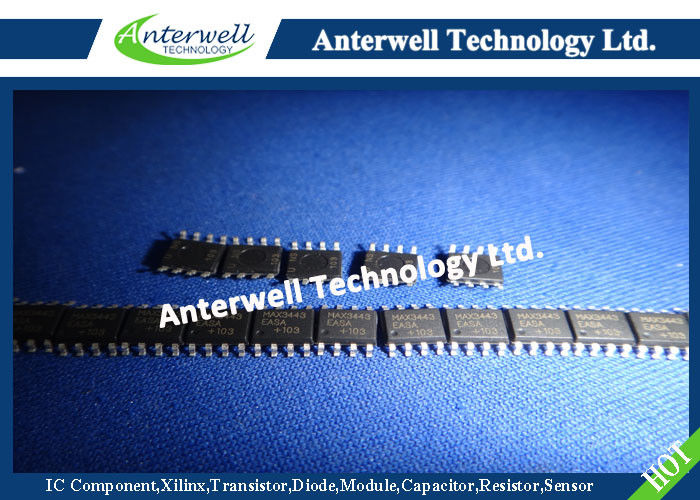
Large Original stock of IC Electronics Components, Transistors, Diodes etc.
High Quality, Reasonable Price, Fast Delivery.
Anterwell Technology Ltd.
Large Original stock of IC Electronics Components, Transistors, Diodes etc.
High Quality, Reasonable Price, Fast Delivery.


Product Details:
Payment & Shipping Terms:
|
| Driver Input High Voltage: | 2.0V | Driver Input Low Voltage: | 0.8V |
|---|---|---|---|
| Driver Input Current: | ±2µA | Driver Output Fault Current: | ±6mA |
| Driver Short-Circuit Output Current: | ±350mA | Driver Short-Circuit Foldback Output Current: | ±25mA |
| Highlight: | programming ic chips,programmable audio chip |
||
±60V Fault-Protected, 10Mbps, Fail-Safe RS-485 Transceiver
with ±15kV ESD Protection
General Description
The MAX3443E fault-protected RS-485/RS-422 transceiver features ±60V protection from signal faults on communication bus lines. Each device contains one differential line driver with three-state output, and one differential line receiver with three-state input. The 1/4-unit-load receiver input impedance allows up to 128 transceivers on a single bus. The device operates from a 5V supply at data rates up to 10Mbps. True fail-safe inputs guarantee a logic-high receiver output when the receiver inputs are open, shorted, or connected to an idle data line.
Hot-swap circuitry eliminates false transitions on the data cable during circuit initialization or connection to a live backplane. Short-circuit current limiting and thermal shutdown circuitry protect the driver against excessive power dissipation, and integrated ±15kV ESD protection eliminates costly external protection devices.
The MAX3443E is available in 8-pin SO and PDIP packages, and is specified over commercial, industrial, and automotive temperature ranges.
Applications
RS-422/RS-485 Communications
Industrial Networks
Telecommunication Systems
Automotive Applications
HVAC Controls
Features
♦ ±60V Fault Protection
♦ ±15kV ESD Protection
♦ Guaranteed 10Mbps Data Rate
♦ Allows Up to 128 Transceivers on the Bus
♦ -7V to +12V Common-Mode Input Range
♦ True Fail-Safe Receiver Inputs
♦ Hot-Swap Inputs for Telecom Applications
♦ Automotive Temperature Range (-40°C to +125°C)
♦ Industry-Standard Pinout
Pin Configuration and Typical Operating Circuit
![]()
ABSOLUTE MAXIMUM RATINGS
All Voltages Referenced with Respect to GND
VCC ........................................................................................+7V
RE, DE, DI...................................................-0.3V to (VCC + 0.3V)
A, B (Note 1) ........................................................................±60V
RO ..............................................................-0.3V to (VCC + 0.3V)
Continuous Power Dissipation (TA = +70°C)
8-Pin SO (derate 5.9mW/°C above +70°C)..................471mW
8-Pin PDIP (derate 9.09mW/°C above +70°C).............727mW
Operating Temperature Ranges
MAX3443EC_ _ ..................................................0°C to +70°C
MAX3443EE_ _ ...............................................-40°C to +85°C
MAX3443EA_ _ .............................................-40°C to +125°C
Storage Temperature Range .............................-65°C to +150°C
Short-Circuit Duration (RO, A, B) ...............................Continuous
Lead Temperature (soldering, 10s) .................................+300°C
Note 1: A, B must be terminated with 54Ω or 100Ω to guarantee ±60V fault protection.
| PARAMETER | SYMBOL | CONDITIONS | MIN TYP MAX | UNITS | |
| DRIVER | |||||
| Differential Driver Output | VOD | Figure 1, RL = 50Ω | 2.0 VCC | V | |
| Figure 1, RL = 27Ω | 1.5 VCC | ||||
|
Change in Magnitude of Differential Output Voltage |
∆VOD | Figure 1, RL = 50Ω or 27Ω (Note 2) | 0.2 | V | |
|
Driver Common-Mode Output Voltage |
VOC | Figure 1, RL = 50Ω or 27Ω | VCC / 2 3 | V | |
|
Change In Magnitude of Common-Mode Voltage |
∆VOC | Figure 1, RL = 50Ω or 27Ω (Note 2) | 0.2 | V | |
| RECEIVER | |||||
| Input Current | IA,B | A,B | DE = GND, VCC = GND, VA, B = +12V | 250 | µA |
| VA, B = -7V | -150 | µA | |||
| VA, B = ±60V | ±6 | mA | |||
|
Receiver Differential Threshold Voltage |
VTH | -7V ≤ VCM ≤ +12V | -200 -50 | mV | |
| Receiver Input Hysteresis | ∆VTH | 25 | mV | ||
| RECEIVER LOGIC | |||||
| Output High Voltage | VOH | Figure 2, IOH = -1.6mA | VCC - 0.6 | V | |
| Output Low Voltage | VOL | Figure 2, IOL = 1mA | 0.4 | V | |
|
Three-State Output Current at Receiver |
IOZR | 0 ≤ VA, B ≤ VCC | ±1 | µA | |
| Receiver Input Resistance | RIN | -7V ≤ VCM ≤ +12V | 48 | kΩ | |
|
Receiver Output Short-Circuit Current |
IOSR | 0 ≤ VRO ≤ VCC | ±95 | mA | |
| CONTROL | |||||
| Control Input High Voltage | VCIH | DE, RE | 2.0 | V | |
|
Input Current DE Current Latch During First DE Rising Edge |
90 | µA | |||
|
Input Current RE Current Latch During First RE Falling Edge |
90 | µA | |||
High Power Rectifier Diode 1N4756A , Silicon Planar Zener Diodes
Bridge Type Rectifier Diode 1N4007 50 to 1000 Volts 1.0 Ampere
1N4742A Silicon Planar Zener Diodes for Stabilized Power Supply
Power Programmable IC Chips XC6SLX100-3FGG484C Spartan-6 Family Overview
128K Bytes Sound IC Chip Programming ATMEGA128-16AU 8 Bit Microcontroller
EMC Programmable IC Chips Compliant Slew Rate Limited EI , Timer IC Chip
SMD Power Mosfet Module L7812CV TO-220 Power Trans Electronic Compoents
2SD1594 3 Pin Transistor NEC NPN Power Transistor Switching High Speed
2N5459 Power Mosfet Transistor N-Channel To-92 Original Stock FSC