Anterwell Technology Ltd.
Anterwell Technology Ltd.
Large Original stock of IC Electronics Components, Transistors, Diodes etc.
High Quality, Reasonable Price, Fast Delivery.
Anterwell Technology Ltd.
Large Original stock of IC Electronics Components, Transistors, Diodes etc.
High Quality, Reasonable Price, Fast Delivery.


Product Details:
Payment & Shipping Terms:
|
| Output Voltage: | Max. 60 V | Output Current (peak-to-peak): | Max. 3 A |
|---|---|---|---|
| Supply Voltage: | Max. 40 V | Guard Circuit Output Voltage: | Max. 5,6 V |
| Operating Ambient Temperature Range: | −25 To +60 °C | Storage Temperature: | −55 To +150 °C |
| High Light: | electronics ic chip,integrated circuit ic |
||
Vertical deflection and guard circuit (110˚)
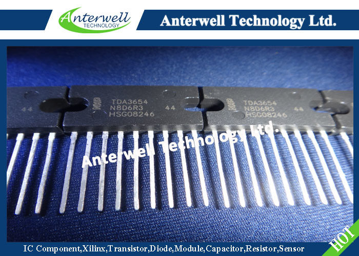
TDA3654
TDA3654Q
GENERAL DESCRIPTION
The TDA3654 is a full performance vertical deflection output circuit for direct drive of the deflection coils and can be used for a wide range of 90° and 110° deflection systems. A guard circuit is provided which blanks the picture tube screen in the absence of deflection current.
Features
• Direct drive to the deflection coils
• 90° and 110° deflection system
• Internal blanking guard circuit
• Internal voltage stabilizer
QUICK REFERENCE DATA
Output voltage V5-2 max. 60 V
Output current (peak-to-peak) I5(p-p) max. 3 A
Supply voltage V9-2 max. 40 V
Guard circuit output voltage V7-2 max. 5,6 V
Operating ambient temperature range Tamb −25 to +60 °C
Storage temperature Tstg −55 to +150 °C
THERMAL RESISTANCE
From junction to mounting base Rth j-mb 3,5 to 4 K/W
PACKAGE OUTLINES
TDA3654 : 9-lead SIL; plastic power (SOT131) .
TDA3654Q : 9-lead SIL bent to DIL; plastic power (SOT157) .
![]()
FUNCTIONAL DESCRIPTION
Output stage and protection circuits
The output stage consists of two Darlington configurations in class B arrangement. Each output transistor can deliver 1,5 A maximum and the VCEO is 60 V.
Protection of the output stage is such that the operation of the transistors remains well within the SOAR area in all circumstances at the output pin, (pin 5). This is obtained by the cooperation of the thermal protection circuit, the current-voltage detector and the short circuit protection.
Special measures in the internal circuit layout give the output transistors extra solidity, this is illustrated in Fig.5 where typical SOAR curves of the lower output transistor are given. The same curves also apply for the upper output device. The supply for the output stage is fed to pin 6 and the output stage ground is connected to pin 4.
Driver and switching circuit
Pin 1 is the input for the driver of the output stage. The signal at pin 1 is also applied to pin 3 which is the input of a switching circuit (pin 1 and 3 are connected via external resistors).
This switching circuit rapidly turns off the lower output stage when the flyback starts and it, therefore, allows a quick start of the flyback generator. The maximum required input signal for the maximum output current peak-to-peak value of 3 A is only 3 V, the sum of the currents in pins 1 and 3 is then maximum 1 mA.
Flyback generator
During scan, the capacitor between pins 6 and 8 is charged to a level which is dependent on the value of the resistor at pin 8 (see Fig.1).
When the flyback starts and the voltage at the output pin (pin 5) exceeds the supply voltage, the flyback generator is activated.
The supply voltage is then connected in series, via pin 8, with the voltage across the capacitor during the flyback period. This implies that during scan the supply voltage can be reduced to the required scan voltage plus saturation voltage of the output transistors.
The amplitude of the flyback voltage can be chosen by changing the value of the external resistor at pin 8. It should be noted that the application is chosen such that the lowest voltage at pin 8 is > 1,5 V, during normal operation.
Guard circuit
When there is no deflection current, for any reason, the voltage at pin 8 becomes less than 1 V, the guard circuit will produce a d.c. voltage at pin 7. This voltage can be used to blank the picture tube, so that the screen will not burn in.
Voltage stabilizer
The internal voltage stabilizer provides a stabilized supply of 6 V to drive the output stage, so the drive current is not affected by supply voltage variations.
RATINGS
Limiting values in accordance with the Absolute Maximum System (IEC 134).
Pins 2 and 4 are externally connected to ground.
Voltages
Output voltage V5-4 0 to 60 V
Supply voltage V9-4 0 to 40 V
Supply voltage output stage V6-4 0 to 60 V
Input voltage V1-2 0 to V9-4 V
Input voltage switching circuit V3-2 0 to V9-4 V
External voltage at pin 7 V7-2 0 to 5,6 V
Currents
Repetitive peak output current ± I5RM max. 1,5 A
Non-repetitive peak output current (note 1) ± I5SM max. 3 A
Repetitive peak output current of flyback generator I8RM max. + 1,5 A
− 1,6 A
Non-repetitive peak output current of flyback generator (note 1) ± I8SM max. 3 A
Temperatures
Storage temperature range Tstg −65 to + 150 °C
Operating ambient temperature range (see Fig.3) Tamb −25 to + 60 °C
Operating junction temperature range Tj −25 to + 150 °C
(the output current at pin 5 should not exceed 2.5A)
High Power Rectifier Diode 1N4756A , Silicon Planar Zener Diodes
Bridge Type Rectifier Diode 1N4007 50 to 1000 Volts 1.0 Ampere
1N4742A Silicon Planar Zener Diodes for Stabilized Power Supply
Power Programmable IC Chips XC6SLX100-3FGG484C Spartan-6 Family Overview
128K Bytes Sound IC Chip Programming ATMEGA128-16AU 8 Bit Microcontroller
EMC Programmable IC Chips Compliant Slew Rate Limited EI , Timer IC Chip
SMD Power Mosfet Module L7812CV TO-220 Power Trans Electronic Compoents
2SD1594 3 Pin Transistor NEC NPN Power Transistor Switching High Speed
2N5459 Power Mosfet Transistor N-Channel To-92 Original Stock FSC