Anterwell Technology Ltd.
Anterwell Technology Ltd.
Large Original stock of IC Electronics Components, Transistors, Diodes etc.
High Quality, Reasonable Price, Fast Delivery.
Anterwell Technology Ltd.
Large Original stock of IC Electronics Components, Transistors, Diodes etc.
High Quality, Reasonable Price, Fast Delivery.
Product Details:
Payment & Shipping Terms:
|
| Storage Temperature: | –65°C To +125°C | Ambient Temperature With Power Applied: | –55°C To +125°C |
|---|---|---|---|
| Output Short Circuit Current: | 200 MA | Input Load Current: | ±1.0 µA |
| A9 Input Load Current: | 50 µA | Output Leakage Current: | ±1.0 µA |
| High Light: | electronic integrated circuit,linear integrated circuits |
||
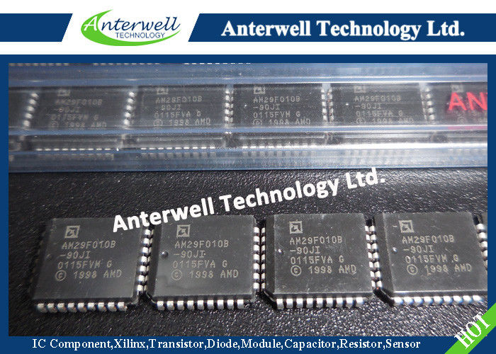
Am29F010B
1 Megabit (128 K x 8-bit)
CMOS 5.0 Volt-only, Uniform Sector Flash Memory
DISTINCTIVE CHARACTERISTICS
■ Single power supply operation
— 5.0 V ± 10% for read, erase, and program operations
— Simplifies system-level power requirements
■ Manufactured on 0.32 µm process technology
— Compatible with Am29F010 and Am29F010A device
■ High performance
— 45 ns maximum access time
■ Low power consumption
— 12 mA typical active read current
— 30 mA typical program/erase current
— <1 µA typical standby current
■ Flexible sector architecture
— Eight 16 Kbyte sectors
— Any combination of sectors can be erased
— Supports full chip erase
■ Sector protection
— Hardware-based feature that disables/reenables program and erase operations
in any combination of sectors
— Sector protection/unprotection can be implemented using standard PROM
programming equipment
■ Embedded Algorithms
— Embedded Erase algorithm automatically pre-programs and erases the chip or
any combination of designated sector
— Embedded Program algorithm automatically programs and verifies data at specified address
■ Erase Suspend/Resume
— Supports reading data from a sector not being erased
■ Minimum 1 million erase cycles guaranteed per sector
■ 20-year data retention at 125°C
— Reliable operation for the life of the system
■ Package options
— 32-pin PLCC
— 32-pin TSOP
— 32-pin PDIP
■ Compatible with JEDEC standards
— Pinout and software compatible with single-power-supply flash
— Superior inadvertent write protection
■ Data# Polling and Toggle Bits
— Provides a software method of detecting program or erase cycle completion
GENERAL DESCRIPTION
The Am29F010B is a 1 Mbit, 5.0 Volt-only Flash memory organized as 131,072 bytes. The Am29F010B is offered in 32-pin PDIP, PLCC and TSOP packages. The byte-wide data appears on DQ0-DQ7. The device is designed to be programmed in-system with the standard system 5.0 Volt VCC supply. A 12.0 volt VPP is not required for program or erase operations. The device can also be programmed or erased in standard EPROM programmers.
This device is manufactured using AMD’s 0.32 µm process technology, and offers all the features and benefits of the Am29F010 and Am29F010A.
The standard device offers access times of 45, 55, 70, 90, and 120 ns, allowing high-speed microprocessors to operate without wait states. To eliminate bus contention the device has separate chip enable (CE#), write enable (WE#) and output enable (OE#) controls.
The device requires only a single 5.0 volt power supply for both read and write functions. Internally generated and regulated voltages are provided for the program and erase operations.
The device is entirely command set compatible with the JEDEC single-power-supply Flash standard. Commands are written to the command register using standard microprocessor write timings. Register contents serve as input to an internal state machine that controls the erase and programming circuitry. Write cycles also internally latch addresses and data needed for the programming and erase operations. Reading data out of the device is similar to reading from other Flash or EPROM devices.
Device programming occurs by executing the program command sequence. This invokes the Embedded Program algorithm—an internal algorithm that automatically times the program pulse widths and verifies proper cell margin.
Device erasure occurs by executing the erase command sequence. This invokes the Embedded Erase algorithm—an internal algorithm that automatically preprograms the array (if it is not already programmed) before executing the erase operation. During erase, the device automatically times the erase pulse widths and verifies proper cell margin.
The host system can detect whether a program or erase operation is complete by reading the DQ7 (Data# Polling) and DQ6 (toggle) status bits. After a program or erase cycle has been completed, the device is ready to read array data or accept another command.
The sector erase architecture allows memory sectors to be erased and reprogrammed without affecting the data contents of other sectors. The device is erased when shipped from the factory.
The hardware data protection measures include a low VCC detector automatically inhibits write operations during power transitions. The hardware sector protection feature disables both program and erase operations in any combination of the sectors of memory, and is implemented using standard EPROM programmers.
The system can place the device into the standby mode. Power consumption is greatly reduced in this mode.
AMD’s Flash technology combines years of Flash memory manufacturing experience to produce the highest levels of quality, reliability, and cost effectiveness. The device electrically erases all bits within a sector simultaneously via Fowler-Nordheim tunneling. The bytes are programmed one byte at a time using the EPROM programming mechanism of hot electron injection.
ABSOLUTE MAXIMUM RATINGS
Storage Temperature (Plastic Packages) . . . . . . . . . . . . . . . –65°C to +125°C
Ambient Temperature with Power Applied. . . . . . . . . . . . . . –55°C to +125°C
Voltage with Respect to Ground
VCC (Note 1). . . . . . . . . . . . . . . . . . . .–2.0 V to +7.0 V
A9 (Note 2). . . . . . . . . . . . . . . . . . . .–2.0 V to +13.0 V
All other pins (Note 1) . . . . . . . . . . . .–2.0 V to +7.0 V
Output Short Circuit Current (Note 3) . . . . . . 200 mA
Notes:
1. Minimum DC voltage on input or I/O pin is –0.5 V. During voltage transitions, inputs may overshoot VSS to –2.0 V for periods of up to 20 ns. See Figure 5. Maximum DC voltage on input and I/O pins is VCC + 0.5 V. During voltage transitions, input and I/O pins may overshoot to VCC + 2.0 V for periods up to 20 ns. See Figure 6.
2. Minimum DC input voltage on A9 pin is –0.5V. During voltage transitions, A9 pins may overshoot VSS to –2.0 V for periods of up to 20 ns. See Figure 5. Maximum DC input voltage on A9 is +12.5 V which may overshoot to 14.0 V for periods up to 20 ns.
3. No more than one output shorted at a time. Duration of the short circuit should not be greater than one second.
Stresses above those listed under “Absolute Maximum Ratings” may cause permanent damage to the device. This is a stress rating only; functional operation of the device at these or any other conditions above those indicated in the operational sections of this specification is not implied. Exposure of the device to absolute maximum rating conditions for extended periods may affect device reliability.
![]()
![]()
Stock Offer (Hot Sell)
| Part No. | Quantity | Brand | D/C | Package |
| STTA106U | 25000 | ST | 14+ | DO-214AA |
| STTH112U | 15000 | ST | 13+ | DO-214AA |
| STTH3010W | 4203 | ST | 11+ | TO-247-2 |
| STTH506FP | 24054 | ST | 16+ | TO-220FP |
| STV0987/TR | 8365 | ST | 16+ | QFN |
| STW13NK100Z | 3745 | ST | 14+ | TO-247 |
| STW34NM60ND | 2636 | ST | 14+ | TO-247 |
| STW45NM60 | 2204 | ST | 16+ | TO-247 |
| SUM110P06-07L-E3 | 4693 | VISHAY | 15+ | TO-263 |
| SVF10N60F | 17664 | SILAN | 16+ | TO-220F |
| SVF6N60F | 17616 | SILAN | 15+ | TO-220F |
| SX1276IMLTRT | 3576 | SEMTECH | 16+ | QFN28 |
| SX34T/R | 43000 | PANJIT | 13+ | DO-214AC |
| SY8133FCC | 16670 | SILERGY | 15+ | SOP-8 |
| SZ-10N27VL | 5030 | SANKEN | 14+ | DO-218 |
| T410-600T | 7085 | ST | 08+ | TO-220 |
| T491B107M010AT | 47000 | KEMET | 16+ | SMD |
| T491X106K050AT | 6306 | KEMET | 10+ | SMD |
| TA8000S | 7925 | TOSHIBA | 13+ | ZIP-9 |
| TA8435HQ | 3630 | TOSHIBA | 16+ | ZIP-25 |
| TAJC107M016RNJ | 8363 | AVX | 16+ | SMD |
| TB2906HQ | 6272 | TOSHIBA | 16+ | ZIP-25 |
| TC1047AVNBTR | 19510 | MICROCHIP | 08+ | SOT-23 |
| TC1232CPA | 16520 | MICROCHIP | 10+ | DIP-8 |
| TC1262-3.3VDBTR | 24125 | MICROCHIP | 15+ | SOT-223 |
| TC1320EOA | 5001 | MICROCHIP | 06+ | SOP-8 |
| TC358778XBG | 2599 | TOSHIBA | 16+ | BGA80 |
| TC4066BF | 12639 | TOSHIBA | 13+ | SOP-14 |
| TC4066BP | 55000 | TOSHIBA | 14+ | DIP-14 |
| TC4069UBF | 6959 | TOSHIBA | 13+ | TSSOP-14 |
High Power Rectifier Diode 1N4756A , Silicon Planar Zener Diodes
Bridge Type Rectifier Diode 1N4007 50 to 1000 Volts 1.0 Ampere
1N4742A Silicon Planar Zener Diodes for Stabilized Power Supply
Power Programmable IC Chips XC6SLX100-3FGG484C Spartan-6 Family Overview
128K Bytes Sound IC Chip Programming ATMEGA128-16AU 8 Bit Microcontroller
EMC Programmable IC Chips Compliant Slew Rate Limited EI , Timer IC Chip
SMD Power Mosfet Module L7812CV TO-220 Power Trans Electronic Compoents
2SD1594 3 Pin Transistor NEC NPN Power Transistor Switching High Speed
2N5459 Power Mosfet Transistor N-Channel To-92 Original Stock FSC