Anterwell Technology Ltd.
Anterwell Technology Ltd.
Large Original stock of IC Electronics Components, Transistors, Diodes etc.
High Quality, Reasonable Price, Fast Delivery.
Anterwell Technology Ltd.
Large Original stock of IC Electronics Components, Transistors, Diodes etc.
High Quality, Reasonable Price, Fast Delivery.
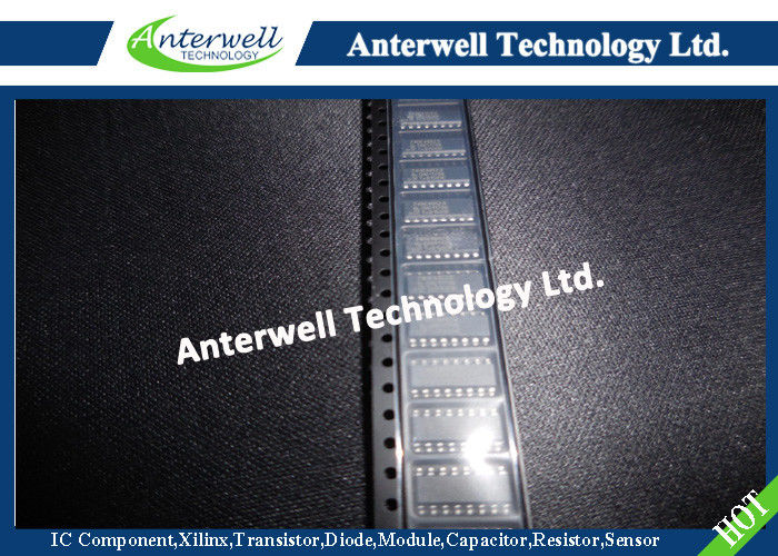
Product Details:
Payment & Shipping Terms:
|
| Supply Voltage: | -0.5 To +11.0 V | Input Diode Current: | ±20 MA |
|---|---|---|---|
| Switch Diode Current: | ±20 MA | Switch Current: | ±25 MA |
| Storage Temperature: | -65 To +150 °C | Power Dissipation: | 500 MW |
| Highlight: | electronic integrated circuit,linear integrated circuits |
||
74HC4052; 74HCT4052
Dual 4-channel analog multiplexer, demultiplexer
FEATURES
• Wide analog input voltage range from −5 V to +5 V
• Low ON-resistance:
– 80 Ω (typical) at VCC − VEE = 4.5 V
– 70 Ω (typical) at VCC − VEE = 6.0 V
– 60 Ω (typical) at VCC − VEE = 9.0 V
• Logic level translation: to enable 5 V logic to communicate with ±5 V analog signals
• Typical “break before make” built in
• Complies with JEDEC standard no. 7A
• ESD protection:
– HBM EIA/JESD22-A114-B exceeds 2000 V
– MM EIA/JESD22-A115-A exceeds 200 V.
• Specified from −40 °C to +85 °C and −40 °C to +125 °C.
APPLICATIONS
• Analog multiplexing and demultiplexing
• Digital multiplexing and demultiplexing
• Signal gating.
DESCRIPTION
The 74HC4052 and 74HCT4052 are high-speed Si-gate CMOS devices and are pin compatible with the HEF4052B. They are specified in compliance with JEDEC standard no. 7A.
The 74HC4052 and 74HCT4052 are dual 4-channel analog multiplexers or demultiplexers with common select logic. Each multiplexer has four independent inputs/outputs (pins nY0 to nY3) and a common input/output (pin nZ). The common channel select logics include two digital select inputs (pins S0 and S1) and an active LOW enable input (pin E). When pin E = LOW, one of the four switches is selected (low-impedance ON-state) with pins S0 and S1. When pin E = HIGH, all switches are in the high-impedance OFF-state, independent of pins S0 and S1.
VCC and GND are the supply voltage pins for the digital control inputs (pins S0, S1, and E). The VCC to GND ranges are 2.0 V to 10.0 V for 74HC4052 and 4.5 V to 5.5 V for 74HCT4052. The analog inputs/outputs (pins nY0 to nY3 and nZ) can swing between VCC as a positive limit and VEE as a negative limit. VCC − VEE may not exceed 10.0 V.
For operation as a digital multiplexer/demultiplexer, VEE is connected to GND (typically ground).
LIMITING VALUES
In accordance with the Absolute Maximum Rating System (IEC 60134); voltages are referenced to VEE = GND (ground = 0 V); note 1.
| SYMBOL | PARAMETER | CONDITIONS | MIN. | MAX. | UNIT |
| VCC | supply voltage | −0.5 | +11.0 | V | |
| IIK | input diode current | VI < −0.5 V or VI > VCC + 0.5 V | − | ±20 | mA |
| ISK | switch diode current | VS < −0.5 V or VS > VCC + 0.5 V | − | ±20 | mA |
| IS | switch current | −0.5 V < VS < VCC + 0.5 V | − | ±25 | mA |
| IEE | VEE current | − | ±20 | mA | |
| ICC; IGND | VCC or GND current | − | ±50 | mA | |
| Tstg | storage temperature | −65 | +150 | °C | |
| Ptot | power dissipation | Tamb = −40 °C to +125 °C; note | − | 500 | mW |
| PS | power dissipation per switch | − | 100 | mW |
Notes
1. To avoid drawing VCC current out of pins nZ, when switch current flows in pins nYn, the voltage drop across the bidirectional switch must not exceed 0.4 V. If the switch current flows into pins nZ, no VCC current will flow out of pins nYn. In this case there is no limit for the voltage drop across the switch, but the voltages at pins nYn and nZ may not exceed VCC or VEE.
2. For DIP16 packages: above 70 °C derate linearly with 12 mW/K.
For SO16 packages: above 70 °C derate linearly with 8 mW/K.
For SSOP16 and TSSOP16 packages: above 60 °C derate linearly with 5.5 mW/K.
For DHVQFN16 packages: above 60 °C derate linearly with 4.5 mW/K.
![]()
Functional diagram
![]()
High Power Rectifier Diode 1N4756A , Silicon Planar Zener Diodes
Bridge Type Rectifier Diode 1N4007 50 to 1000 Volts 1.0 Ampere
1N4742A Silicon Planar Zener Diodes for Stabilized Power Supply
Power Programmable IC Chips XC6SLX100-3FGG484C Spartan-6 Family Overview
128K Bytes Sound IC Chip Programming ATMEGA128-16AU 8 Bit Microcontroller
EMC Programmable IC Chips Compliant Slew Rate Limited EI , Timer IC Chip
SMD Power Mosfet Module L7812CV TO-220 Power Trans Electronic Compoents
2SD1594 3 Pin Transistor NEC NPN Power Transistor Switching High Speed
2N5459 Power Mosfet Transistor N-Channel To-92 Original Stock FSC