Anterwell Technology Ltd.
Anterwell Technology Ltd.
Large Original stock of IC Electronics Components, Transistors, Diodes etc.
High Quality, Reasonable Price, Fast Delivery.
Anterwell Technology Ltd.
Large Original stock of IC Electronics Components, Transistors, Diodes etc.
High Quality, Reasonable Price, Fast Delivery.
Product Details:
Payment & Shipping Terms:
|
| Storage Temperature: | –65°C To +150°C | Ambient Temperature With Power Applied: | –55°C To +125°C |
|---|---|---|---|
| Supply Voltage To Ground Potential: | –0.5V To +7.0V | DC Input Voltage: | –0.5V To +7.0V |
| Power Dissipation: | 1.0W | Output Current, Into Outputs (LOW): | 20 MA |
| Highlight: | electronic integrated circuit,linear integrated circuits |
||
Stock Offer (Hot Sell)
| Part no. | Quantity | Brand | D/C | Package |
| CS4344-CZZR | 3800 | CIRRUS | 16+ | MSOP |
| LTC1844ES5-3.3 | 3800 | LINEAR | 16+ | SOT23-5 |
| MC33039P | 3800 | ON | 13+ | DIP-8 |
| MMA7660FCR1 | 3800 | FREESCALE | 15+ | DFN-10 |
| NLV32T-100J-PF | 3800 | TDK | 16+ | SMD |
| PC401 | 3800 | SHARP | 16+ | SOP-5 |
| SN75179BP | 3800 | TI | 14+ | DIP8 |
| STP10NK70ZFP | 3800 | ST | 14+ | TO-220 |
| UC3842BD1R2G | 3800 | ON | 14+ | SOP-8 |
| LM393DR | 3810 | TI | 16+ | SOP8 |
| BZX84-C18 | 3820 | NXP | 16+ | SOT-23 |
| LPC2136FBD64 | 3820 | NXP | 13+ | TQFP-64 |
| LP3982IMMX-2.5 | 3821 | NS | 15+ | MSOP8 |
| TOP224PN | 3821 | POWER | 16+ | DIP-8 |
| TLP121 | 3822 | TOSHIBA | 16+ | SOP-4 |
| IRF4905 | 3870 | IR | 14+ | TO-220 |
| MC3403 | 3870 | ON | 14+ | SOP-14 |
| P2504EDG | 3870 | INKO | 14+ | TO-252 |
| STB16NS25 | 3870 | ST | 16+ | TO-263 |
| SSM3K7002FU | 3871 | TOSHIBA | 16+ | SOT323 |
| 3122V | 3880 | SANYO | 13+ | TO-3P |
| CD4017BCN | 3880 | NSC | 15+ | DIP |
| MIC842LYC5 | 3880 | MICREL | 16+ | SC70-5 |
| IMZ2A | 3887 | ROHM | 16+ | SOT-163 |
| EPCS4SI8N | 3888 | ALTERA | 14+ | SOP-8 |
| SN74LVC1T45DCK | 3888 | TI | 14+ | SC-70-6 |
| UCC2813D-2 | 3888 | TI | 14+ | SOP8 |
| 2SC4552 | 3900 | NEC | 16+ | TO-220 |
| MC14551BDR2G | 3900 | ON | 16+ | SOP16 |
| MX29LV040CQC-70G | 3900 | MXIC | 13+ | PLCC |
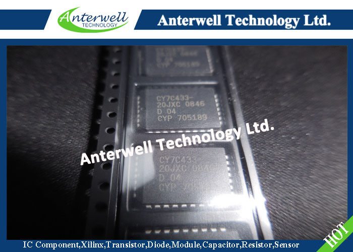
CY7C419/21/25/29/33
256/512/1K/2K/4K x 9 Asynchronous FIFO
Features
• Asynchronous first-in first-out (FIFO) buffer memories
• 256 x 9 (CY7C419)
• 512 x 9 (CY7C421)
• 1K x 9 (CY7C425)
• 2K x 9 (CY7C429)
• 4K x 9 (CY7C433)
• Dual-ported RAM cell
• High-speed 50.0-MHz read/write independent of depth/width
• Low operating power: ICC = 35 mA
• Empty and Full flags (Half Full flag in standalone)
• TTL compatible
• Retransmit in standalone
• Expandable in width
• PLCC, 7x7 TQFP, SOJ, 300-mil and 600-mil DIP
• Pb-Free Packages Available
• Pin compatible and functionally equivalent to IDT7200, IDT7201, IDT7202, IDT7203, IDT7204, AM7200, AM7201, AM7202, AM7203, and AM7204
Functional Description
The CY7C419, CY7C420/1, CY7C424/5, CY7C428/9, and CY7C432/3 are first-in first-out (FIFO) memories offered in 600-mil wide and 300-mil wide packages. They are, respectively, 256, 512, 1,024, 2,048, and 4,096 words by 9-bits wide. Each FIFO memory is organized such that the data is read in the same sequential order that it was written. Full and Empty flags are provided to prevent overrun and underrun. Three additional pins are also provided to facilitate unlimited expansion in width, depth, or both. The depth expansion technique steers the control signals from one device to another in parallel, thus eliminating the serial addition of propagation delays, so that throughput is not reduced. Data is steered in a similar manner.
The read and write operations may be asynchronous; each can occur at a rate of 50.0 MHz. The write operation occurs when the write (W) signal is LOW. Read occurs when read (R) goes LOW. The nine data outputs go to the high-impedance state when R is HIGH.
A Half Full (HF) output flag is provided that is valid in the standalone and width expansion configurations. In the depth expansion configuration, this pin provides the expansion out (XO) information that is used to tell the next FIFO that it will be activated.
In the standalone and width expansion configurations, a LOW on the retransmit (RT) input causes the FIFOs to retransmit the data. Read enable (R) and write enable (W) must both be HIGH during retransmit, and then R is used to access the data.
The CY7C419, CY7C420, CY7C421, CY7C424, CY7C425, CY7C428, CY7C429, CY7C432, and CY7C433 are fabricated using an advanced 0.65-micron P-well CMOS technology. Input ESD protection is greater than 2000V and latch-up is prevented by careful layout and guard rings.
Maximum Rating[1]
(Above which the useful life may be impaired. For user guidelines, not tested.)
Storage Temperature .................................–65°C to +150°C
Ambient Temperature with
Power Applied.............................................–55°C to +125°C
Supply Voltage to Ground Potential ............... –0.5V to +7.0V
DC Voltage Applied to Outputs
in High Z State................................................–0.5V to +7.0V
DC Input Voltage ............................................–0.5V to +7.0V
Power Dissipation.......................................................... 1.0W
Output Current, into Outputs (LOW)............................ 20 mA
Static Discharge Voltage............................................ >2000V
(per MIL–STD–883, Method 3015)
Latch-Up Current..................................................... >200 mA
Note: 1. Single Power Supply: The voltage on any input or I/O pin can not exceed the power pin during power-up.
Operating Range
| Range | Ambient Temperature[2] | VCC |
| Commercial | 0°C to + 70°C | 5V ± 10% |
| Industrial | –40°C to +85°C | 5V ± 10% |
| Military | –55°C to +125°C | 5V ± 10% |
![]()
High Power Rectifier Diode 1N4756A , Silicon Planar Zener Diodes
Bridge Type Rectifier Diode 1N4007 50 to 1000 Volts 1.0 Ampere
1N4742A Silicon Planar Zener Diodes for Stabilized Power Supply
Power Programmable IC Chips XC6SLX100-3FGG484C Spartan-6 Family Overview
128K Bytes Sound IC Chip Programming ATMEGA128-16AU 8 Bit Microcontroller
EMC Programmable IC Chips Compliant Slew Rate Limited EI , Timer IC Chip
SMD Power Mosfet Module L7812CV TO-220 Power Trans Electronic Compoents
2SD1594 3 Pin Transistor NEC NPN Power Transistor Switching High Speed
2N5459 Power Mosfet Transistor N-Channel To-92 Original Stock FSC