Anterwell Technology Ltd.

          Anterwell Technology Ltd.


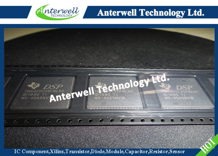
Large Original stock of IC Electronics Components, Transistors, Diodes etc.

High Quality, Reasonable Price, Fast Delivery.

Home
Products
About Us
Factory Tour
Quality Control
Contact Us
Request A Quote
Home ProductsElectronic IC Chips

TMS320C25FNL50 Integrated Circuit Chip TMS320 SECOND GENERATION DIGITAL SIGNAL PROCESSORS

Good quality Programmable IC Chips for sales
We have cooperate with Anterwell near 7 years. always very good quality good service. Original and very fast delivery. A very good partner.

—— Clemente From Brzail

I'm doing business with Anterwell from 2006, from small to big orders. Reliable!

—— Ingalill From Sweden

Sharon is a very good girl, we are very happy to cooperate with her. Competitive price and professional. Never have quality problem with them.

—— Alfredo From USA

We always buy XILINX parts from Anterwell. High quality with good price. Hope can have more business with you.

—— Mr Babak From Iran

I'm Online Chat Now

TMS320C25FNL50 Integrated Circuit Chip TMS320 SECOND GENERATION DIGITAL SIGNAL PROCESSORS

China TMS320C25FNL50 Integrated Circuit Chip TMS320 SECOND GENERATION DIGITAL SIGNAL PROCESSORS supplier

Large Image :  TMS320C25FNL50 Integrated Circuit Chip TMS320 SECOND GENERATION DIGITAL SIGNAL PROCESSORS

Product Details:

Place of Origin: original factory
Brand Name: Anterwell
Certification: new & original
Model Number: TMS320C25FNL50

Payment & Shipping Terms:

Minimum Order Quantity: 10pcs
Price: Negotiate
Packaging Details: Please contact me for details
Delivery Time: 1 day
Payment Terms: T/T, Western Union, Paypal
Supply Ability: 4200pcs
Contact Now
Detailed Product Description
Supply Voltage: -0.3 V To 7 V Input Voltage: -0.3 V To 15 V
Output Voltage: - 0.3 V To 7 V Continuous Power Dissipation: 1.5 W
Operating Free-air Temperature Range: 0℃ To 70℃ Storage Temperature Range: -55℃ To 150℃
High Light:

digital integrated circuits

,

linear integrated circuits


  • 80-ns Instruction Cycle Time
  • 544 Words of On-Chip Data RAM
  • 4K Words of On-Chip Secure Program EPROM (TMS320E25)
  • 4K Words of On-Chip Program ROM (TMS320C25)
  • 128K Words of Data/Program Space
  • 32-Bit ALU/Accumulator
  • 16 * 16-Bit Multiplier With a 32-Bit Product
  • Block Moves for Data/Program Management
  • Repeat Instructions for Efficient Use of Program Space
  • Serial Port for Direct Codec Interface
  • Synchronization Input for Synchronous Multiprocessor Configurations
  • Wait States for Communication to Slow Off-Chip Memories/Peripherals
  • On-Chip Timer for Control Operations
  • Single 5-V Supply
  • Packaging: 68-Pin PGA, PLCC, and CER-QUAD
  • 68-to-28 Pin Conversion Adapter Socket for EPROM Programming
  • Commercial and Military Versions Available
  • NMOS Technology:
    • — TMS32020 ......... 200-ns cycle time 
  • CMOS Technology:
    • — TMS320C25 ........100-ns cycle time 
    • — TMS320E25 ........ 100-ns cycle time
    • — TMS320C25-50 .....80-ns cycle time


description

This data sheet provides complete design documentation for the second-generation devices of the TMS320 family. This facilitates the selection of the devices best suited for user applications by providing all specifications and special features for each TMS320 member. This data sheet is divided into four major sections: architecture, electrical specifications (NMOS and CMOS), timing diagrams, and mechanical data. In each of these sections, generic information is presented first, followed by specific device information. An index is provided for quick reference to specific information about a device.


68-Pin GB Package† (Top View)                              68-Pin FN and FZ Packages† (Top View)

TMS320C25FNL50 Integrated Circuit Chip TMS320 SECOND GENERATION DIGITAL SIGNAL PROCESSORSTMS320C25FNL50 Integrated Circuit Chip TMS320 SECOND GENERATION DIGITAL SIGNAL PROCESSORS


Key Features: TMS32020 TMS320C25FNL50 Integrated Circuit Chip TMS320 SECOND GENERATION DIGITAL SIGNAL PROCESSORS

  • 200-ns Instruction Cycle Time
  • 544 Words of On-Chip Data RAM
  • 128K Words of Total Data/Program Memory Space
  • Wait States for Communication to Slower Off-Chip Memories
  • Source Code Compatible With the TMS320C1x
  • Single-Cycle Multiply/Accumulate Instructions
  • Repeat Instructions
  • Global Data Memory Interface
  • Block Moves for Data/Program Management
  • Five Auxiliary Registers With Dedicated Arithmetic Unit
  • Serial Port for Multiprocessing or Interfacing to Codecs, Serial Analog-to-Digital Converters, etc.
  • On-Chip Clock Generator
  • Single 5-V Supply
  • NMOS Technology
  • 68-Pin Grid Array (PGA) Package


Key Features: TMS320C25, TMS320C25-50, TMS320E25 TMS320C25FNL50 Integrated Circuit Chip TMS320 SECOND GENERATION DIGITAL SIGNAL PROCESSORS

  • 80-ns Instruction Cycle Time (TMS320C25-50)
  • 100-ns Instruction Cycle Time (TMS320C25)
  • 4K Words of On-Chip Secure Program EPROM (TMS320E25)
  • 4K Words of On-Chip Program ROM (TMS320C25)
  • 544 Words of On-Chip RAM
  • 128K Words of Total Program/Data Memory Space
  • Wait States for Communications to Slower Off-Chip Memories
  • Object-Code Compatible With the TMS32020
  • Source-Code Compatible With TMS320C1x
  • 24 Additional Instructions to Support Adaptive Filtering, FFTs, and Extended-Precision Arithmetic
  • Block Moves for Data/Program Management
  • Single-Cycle Multiply/Accumulate Instructions
  • Eight Auxiliary Registers With Dedicated Arithmetic Unit
  • Bit-Reversed Indexed-Addressing Mode for Radix-2 FFTS
  • Double-Buffered Serial Port
  • On-Chip Clock Generator
  • Single 5-V Supply
  • Internal Security Mechanism (TMS320E25)
  • 68-to-28 Pin Conversion Adapter Socket
  • CMOS Technology
  • 68-Pin Grid Array (PGA) Package (TMS320C25)
  • 68-Lead Plastic Leaded Chip Carrier (PLCC) Package (TMS320C25, TMS320C25-50)
  • 68-Lead CER-QUAD Package (TMS320E25)


absolute maximum ratings over specified temperature range (unless otherwise noted)†


Supply voltage range, VCC‡ .......................................................  -0.3 V to 7 V

Input voltage range: TMS320E25 pins 24 and 25..........................-0.3 V to 15 V

                                 All other inputs ..............................................-0.3 V to 7 V

Output voltage range .................................................................... -0.3 V to 7 V

Continuous power dissipation ............................................................. 1.5 W

Operating free-air temperature range  ............................................0℃ to 70℃

Storage temperature range  .......................................................... -55℃ to 150℃


† Stresses beyond those listed under “Absolute Maximum Ratings” may cause permanent damage to the device. This is a stress rating only, and functional operation of the device at these or any other conditions beyond those indicated in the “Recommended Operating Conditions” section of this specification is not implied. Exposure to absolute-maximum-rated conditions for extended periods may affect device reliability.

‡ All voltage values are with respect to VSS.


Contact Details
Anterwell Technology Ltd.

Contact Person: Miss. Sharon Yang

Tel: 86-755-61169882

Fax: 86-755-613169859

Send your inquiry directly to us (0 / 3000)