Anterwell Technology Ltd.

          Anterwell Technology Ltd.


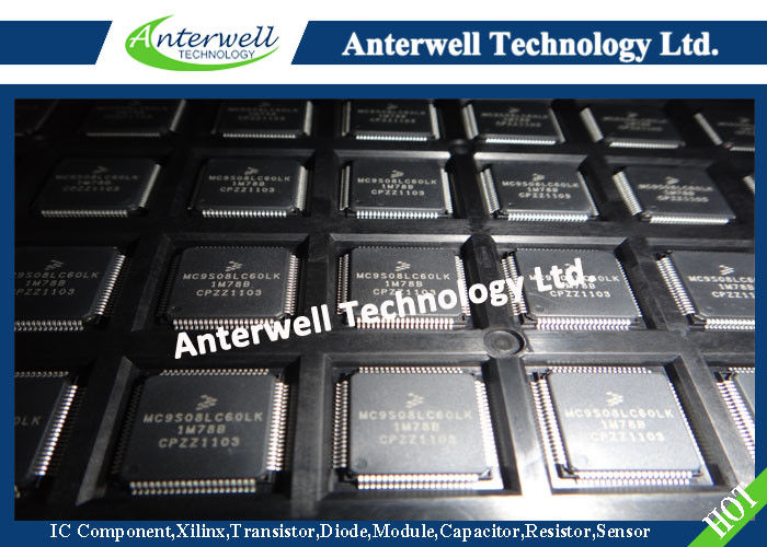
Large Original stock of IC Electronics Components, Transistors, Diodes etc.

High Quality, Reasonable Price, Fast Delivery.

Home
Products
About Us
Factory Tour
Quality Control
Contact Us
Request A Quote
Home ProductsElectronic IC Chips

MC9S08LC60LK Integrated Circuit Chip New & Original Microcontrollers

Good quality Programmable IC Chips for sales
We have cooperate with Anterwell near 7 years. always very good quality good service. Original and very fast delivery. A very good partner.

—— Clemente From Brzail

I'm doing business with Anterwell from 2006, from small to big orders. Reliable!

—— Ingalill From Sweden

Sharon is a very good girl, we are very happy to cooperate with her. Competitive price and professional. Never have quality problem with them.

—— Alfredo From USA

We always buy XILINX parts from Anterwell. High quality with good price. Hope can have more business with you.

—— Mr Babak From Iran

I'm Online Chat Now

MC9S08LC60LK Integrated Circuit Chip New & Original Microcontrollers

China MC9S08LC60LK Integrated Circuit Chip New & Original Microcontrollers supplier

Large Image :  MC9S08LC60LK Integrated Circuit Chip New & Original Microcontrollers

Product Details:

Place of Origin: original factory
Brand Name: Anterwell
Certification: new & original
Model Number: MC9S08LC60LK

Payment & Shipping Terms:

Minimum Order Quantity: 10pcs
Price: Negotiate
Packaging Details: Please contact me for details
Delivery Time: 1 day
Payment Terms: T/T, Western Union, Paypal
Supply Ability: 4200pcs
Contact Now
Detailed Product Description
Supply Voltage: –0.3 To +3.8 V Maximum Current Into VDD: 120 MA
Digital Input Voltage: –0.3 To VDD + 0.3 V Instantaneous Maximum Current: ± 25 MA
Storage Temperature Range: –55 To 150 °C Operating Temperature: -40 To 85 °C
High Light:

digital integrated circuits

,

linear integrated circuits


MC9S08LC60 Features


8-Bit HCS08 Central Processor Unit (CPU)

  • 40-MHz HCS08 CPU
  • HC08 instruction set with added BGND instruction
  • Background debugging system
  • Breakpoint capability to allow single breakpoint setting during in-circuit debugging (plus two more breakpoints in on-chip debug module)
  • In-Circuit Emulator (ICE) debug module containing two comparators and nine trigger modes. Eight deep FIFO for storing change-of-flow addresses and event-only data. ICE debug module supports both tag and force breakpoints.
  • Support for up to 32 interrupt/reset sources


Memory Options

  • Dual on-chip in-circuit programmable FLASH memories with block protection and security options; 60K and 36K options available
  • Program/erase of one FLASH array while executing from another
  • On-chip random-access memory (RAM); 4K and 2.5K options available


Power-Saving Features

  • Wait plus three stops
  • Software disable of clock monitor and low-voltage interrupt (LVI) for lowest stop current
  • Software-generated real-time clock (RTC) functions using real-time interrupt (RTI)


Configurable Clock Source

  • Clock source options include crystal, resonator, external clock, or internally generated clock with precision nonvolatile memory (NVM) trimming
  • Automatic clock monitor function


System Protection

  • Optional computer operating properly (COP) reset
  • Low-voltage detection with reset or interrupt
  • Illegal opcode detection with reset


Package Options

  • 64-pin low-profile quad flat package (LQFP)
  • 80-pin LQFP


Peripherals

  • LCD (liquid crystal display driver) — Compatible with 5-V or 3-V LCD glass displays; functional in wait and stop3 low-power modes; selectable frontplane and backplane configurations:
    • – 4 x 40 or 3 x 41 (80-pin package)
    • – 4 x 32 or 3 x 33 (64-pin package)
  • ACMP (analog comparator) — option to compare to internal reference voltage; output is software selectable to be driven to the input capture of TPM1 channel 0.
  • ADC (analog-to-digital converter) — 8-channel, 12- bit with automatic compare function, asynchronous clock source, temperature sensor and internal bandgap reference channel. ADC is hardware triggerable using the RTI counter.
  • SCI (serial communications interface) — available single-wire mode
  • SPI1 and SPI2 — Two serial peripheral interface modules
  • KBI — Two 8-pin keyboard interrupt modules with software selectable rising or falling edge detect
  • IIC — Inter-integrated circuit bus module capable of operation up to 100 kbps with maximum bus loading; capable of higher baudrates with reduced loading
  • TPM1 and TPM2 — Two timer/pulse-width modulators with selectable input capture, output compare, and edge-aligned PWM capability on each channel. Each timer module may be configured for buffered, centered PWM (CPWM) on all channels.


Input/Output

  • Up to 24 general-purpose input/output (I/O) pins; includes two output-only pins and one input-only pin
  • Software selectable pullups on ports when used as input. Selection is on an individual port bit basis.
  • Software selectable slew rate control on ports when used as outputs (selection is on an individual port bit basis)
  • Software selectable drive strength control on ports when used as outputs (selection is on an individual port bit basis)
  • Internal pullup on RESET and IRQ pin to reduce customer system cost


Absolute Maximum Ratings

                         Rating    Symbol        Value    Unit
  Supply voltage    VDD   –0.3 to +3.8     V
  Maximum current into VDD    IDD          120     mA
  Digital input voltage    VIn   –0.3 to VDD + 0.3     V

  Instantaneous maximum current

     Single pin limit (applies to all port pins)(1), (2), (3)

   ID           ± 25     mA
  Storage temperature range    Tstg    –55 to 150     °C
  1. Input must be current limited to the value specified. To determine the value of the required current-limiting resistor, calculate resistance values for positive (VDD) and negative (VSS) clamp voltages, then use the larger of the two resistance values.
  2. All functional non-supply pins are internally clamped to VSS and VDD.
  3. Power supply must maintain regulation within operating VDD range during instantaneous and operating maximum current conditions. If positive injection current (VIn > VDD) is greater than IDD, the injection current may flow out of VDD and could result in external power supply going out of regulation. Ensure external VDD load will shunt current greater than maximum injection current. This will be the greatest risk when the MCU is not consuming power. Examples are: if no system clock is present, or if the clock rate is very low which would reduce overall power consumption.


Figure 1. MC9S08LC60 Series in 80-Pin LQFP Package

MC9S08LC60LK Integrated Circuit Chip New & Original Microcontrollers


Figure 2. MC9S08LC60 Series in 64-Pin LQFP Package

MC9S08LC60LK Integrated Circuit Chip New & Original Microcontrollers

Note: VREFH/VREFL are internally connected to VDDAD/VSSAD in the 64-pin package.


Contact Details
Anterwell Technology Ltd.

Contact Person: Miss. Sharon Yang

Tel: 86-755-61169882

Fax: 86-755-613169859

Send your inquiry directly to us (0 / 3000)